Electric potential switching device

A switcher and potential technology, applied in the direction of electrical components, electric pulse generation, logic circuit connection/interface layout, etc., to achieve the effect of low transmission delay and low power consumption

Active Publication Date: 2008-07-23
FARADAY TECH CORP
View PDF1 Cites 4 Cited by
  • Summary
  • Abstract
  • Description
  • Claims
  • Application Information

AI Technical Summary

Problems solved by technology

[0010] The object of the present invention is to provide a potential switcher with low power consumption and low transfer delay, so as to overcome the transfer delay and high power consumption in the above-mentioned prior art defect

Method used


Image

  • Electric potential switching device
  • Electric potential switching device
  • Electric potential switching device

Examples


Embodiment Construction

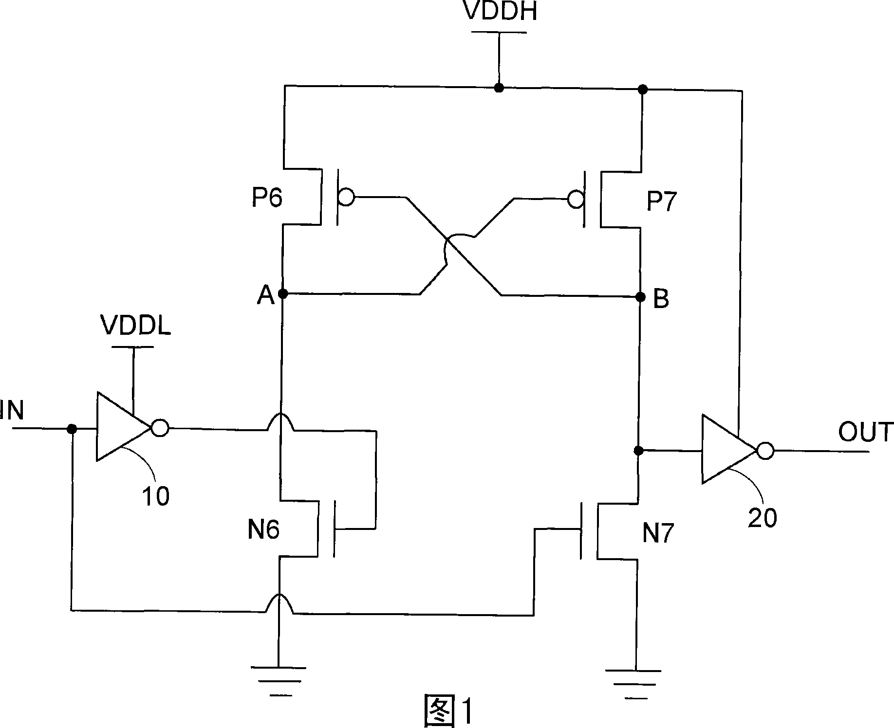
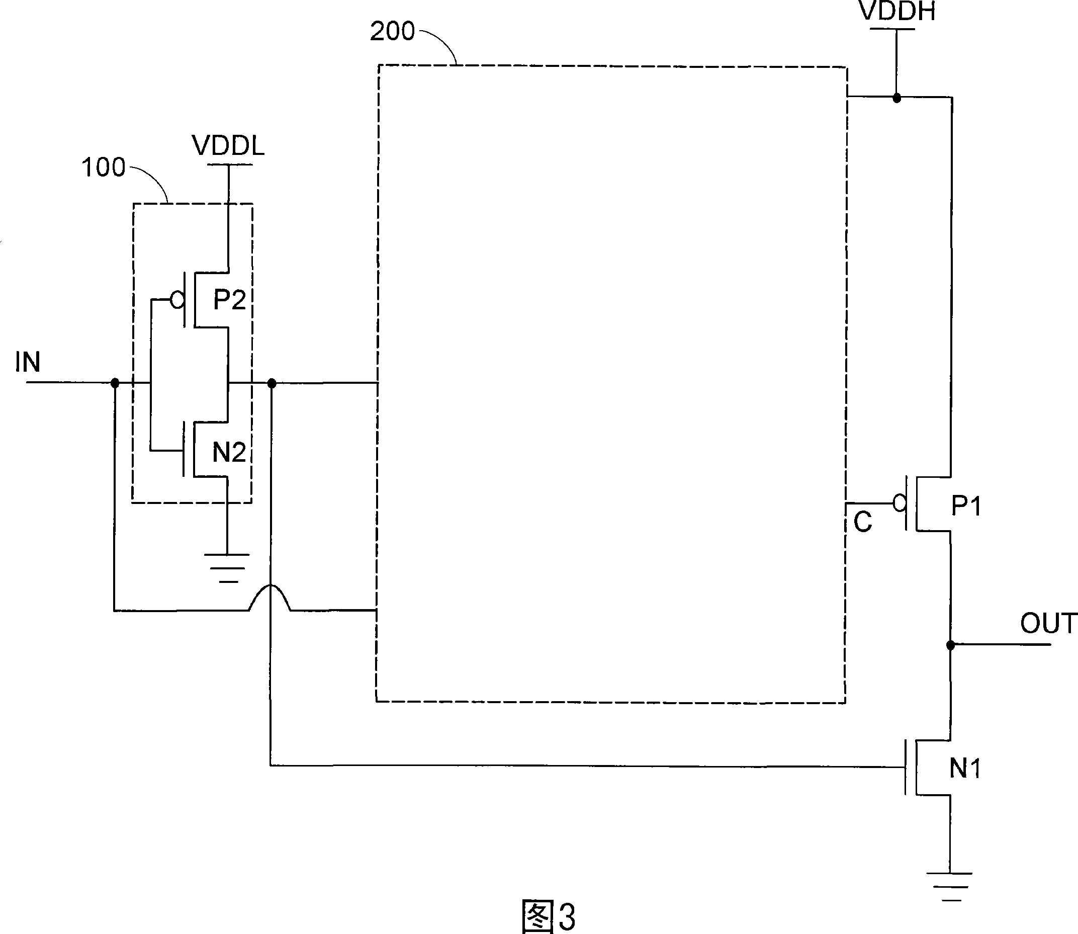
[0042] Please refer to FIG. 3 , which illustrates the potential switcher of the present invention. The potential switch includes: a NOT gate 100, a control circuit 200, a first PMOS transistor (P1) and a first NMOS transistor (N1). Wherein, the signal input terminal (IN) is connected to the input terminal of the NOT gate 100 . The NOT gate 100 includes: the source of the second PMOS transistor (P2) is connected to the low voltage source (VDDL), and the gate of the second PMOS transistor (P2) is connected to the signal input terminal (IN). The drain of the second NMOS transistor (N2) is connected to the drain of the second PMOS transistor (P2), the gate of the second NMOS transistor (N2) is connected to the signal input terminal (IN), and the second NMOS transistor (N2) ) source is connected to this ground terminal. Furthermore, since the NOT gate 100 is connected to the low voltage source (VDDL) and can operate between the first high potential and the low potential. Therefo...


PUM


Abstract

The invention relates to a potential switcher, which comprises a negater which is connected on a first voltage source, wherein the negater can be operated between a first electropositive potential and electronegative potential, and the input end of the negater is connected to the signal input end, a first PMOS transistor whose source cathode is connected with a second voltage source and grid electrode is connected with the controlling end, a first NMOS transistor whose drain electrode is connected with the drain electrode of the first PMOS and is used as signal output end, grid electrode is connected with the output end of the negater, and source cathode is connected with the reference potential, and a controlling circuit which is connected with the signal input end, the output end of the negater and the second voltage source, and the controlling end of the controlling circuit can open the first PMOS transistor, the signal output end is led to output the second electropositive potential, and the controlling end closes the first PMOS transistor, the signal output end is led to output the electronegative potential. The potential switcher of the invention has the advantages of low potential switcher and low transmission delay.

Description

technical field [0001] The invention relates to a potential switcher, in particular to a potential switcher with low power consumption and low propagation delay. Background technique [0002] Generally, potential switches are used between circuits with different voltage sources. That is to say, the use of the potential switch can enable the circuit of two different voltage sources to transmit signals. [0003] Please refer to FIG. 1 , which shows a known potential switcher. The potential switcher includes a sixth PMOS transistor (P6), a seventh PMOS transistor (P7), a sixth NMOS transistor (N6), a seventh NMOS transistor (N7), a first NOT gate (Not gate) 10, and a second NOT gate 20. [0004] The level switcher belongs to the design of cross coupled level converter (CCLC). Wherein, the sources of the sixth PMOS transistor (P6) and the seventh PMOS transistor (P7) are connected to the high voltage source (VDDH), the gate of the sixth PMOS transistor (P6) is connected to t...

Claims


Application Information

Patent Timeline
Patent Type & Authority Applications(China)
IPC IPC(8): H03K3/037H03K3/356H03K19/0185
Inventor 杨智文陈省华
Owner FARADAY TECH CORP
Why Eureka
Try Eureka