Method and system for driving a light emitting device display

A technology for light-emitting devices and displays, applied in static indicators, instruments, etc., can solve the problems of high power consumption, inability to use large-area displays, and high implementation costs

Active Publication Date: 2008-07-23
IGNIS INNOVATION
View PDF0 Cites 16 Cited by
  • Summary
  • Abstract
  • Description
  • Claims
  • Application Information

AI Technical Summary

Problems solved by technology

[0006] However, since V T The generation cycle "VT-GEN" requires a large time budget to generate accurate threshold voltages for driving TFTs, so this timing schedule cannot be used for large area di

Method used


Image

  • Method and system for driving a light emitting device display
  • Method and system for driving a light emitting device display
  • Method and system for driving a light emitting device display

Examples


Embodiment Construction

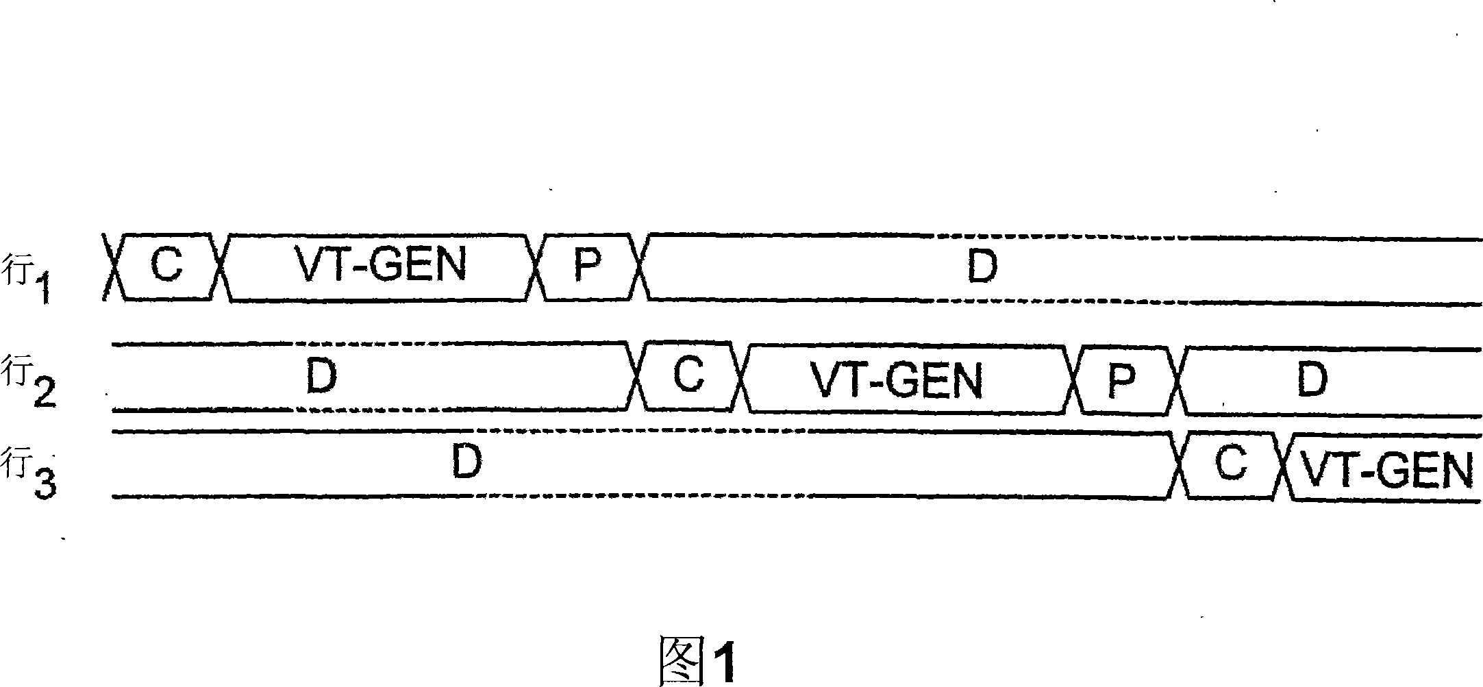
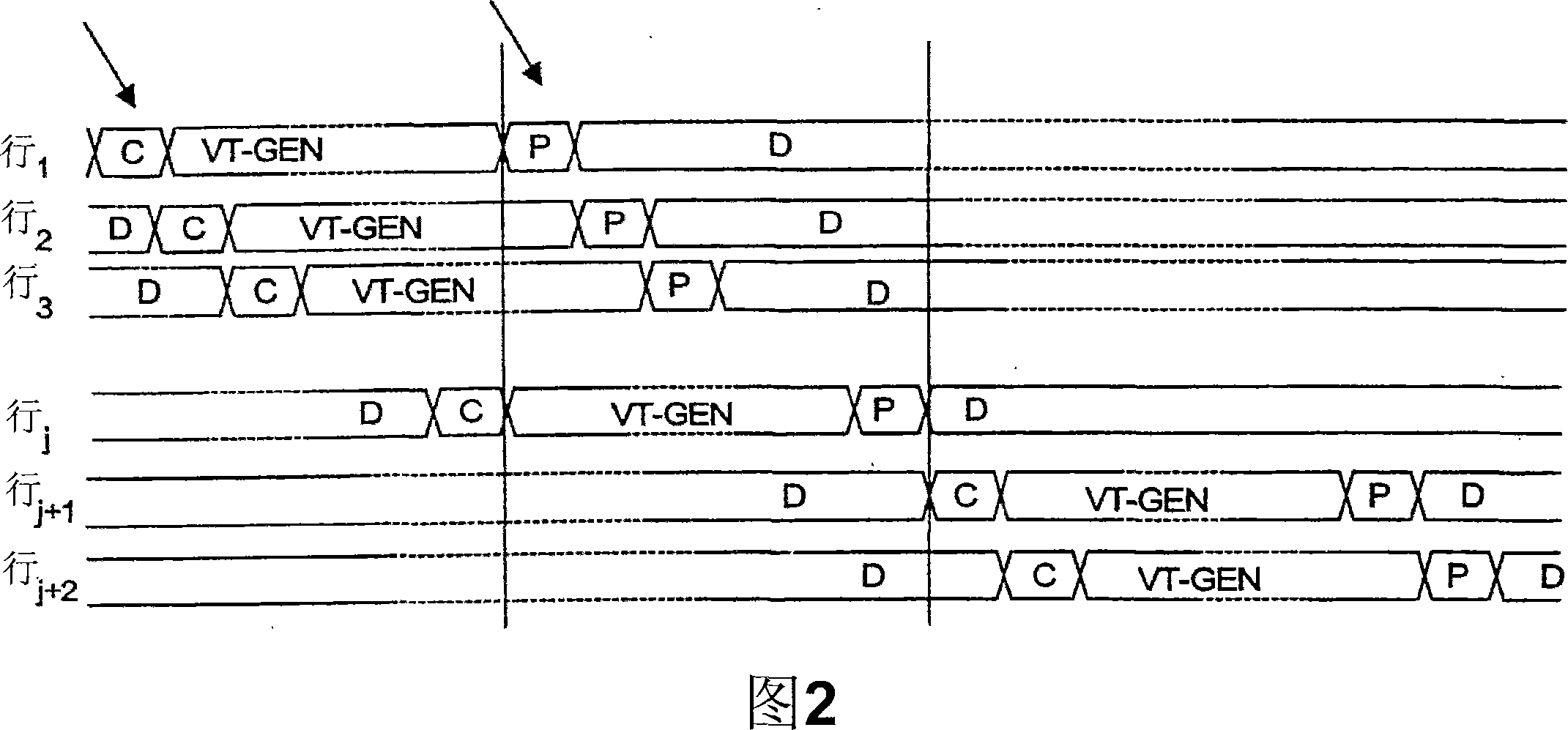
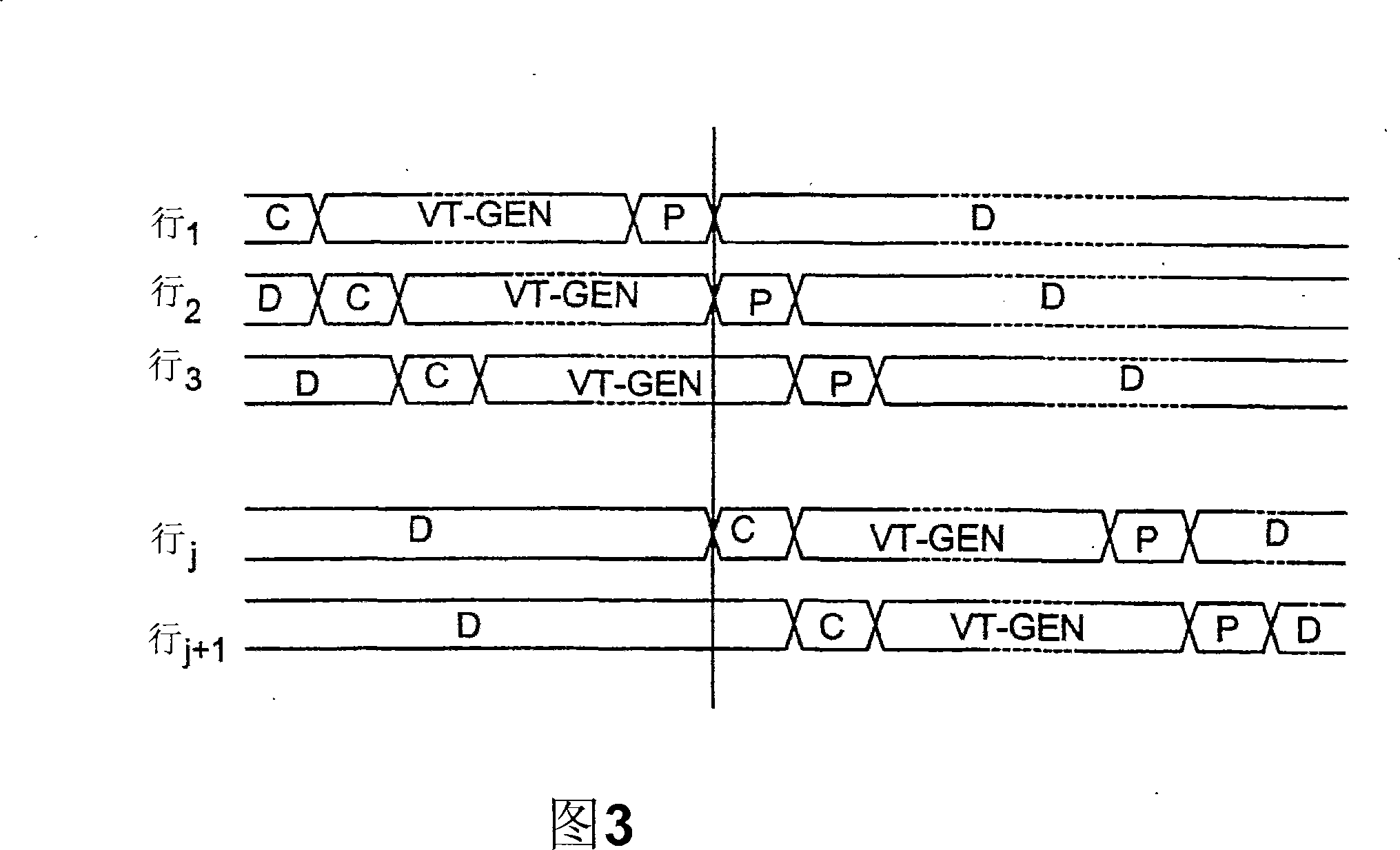
[0036] This disclosure describes an embodiment that utilizes a pixel circuit having a light emitting device, such as an organic light emitting diode (OLED), and a plurality of transistors, such as thin film transistors ( thin filmtransistors, TFT) and the like, arranged in rows and columns to form an AMOLED display. The pixel circuitry may include a pixel driver for the OLED. However, a pixel may include any light emitting device other than an OLED, and a pixel may include any transistor other than a TFT. The transistors in the pixel circuit can be N-type transistors, P-type transistors or combinations thereof. The transistors in the pixels may utilize amorphous silicon, nano / microcrystalline silicon, poly silicon, organic semiconductor technology (eg organic TFT), NMOS / PMOS technology or CMOS technology (eg MOSFET). In the specification, "pixel circuit" and "pixel" are used interchangeably. A pixel circuit may be a current-programmed pixel or a voltage-programmed pixel, an...


PUM


Abstract

A method and system for driving a light emitting device display is provided. The system provides a timing schedule which increases accuracy in the display. The system may provide the timing schedule by which an operation cycle is implemented consecutively in a group of rows. The system may provide the timing schedule by which an aging factor is used for a plurality of frames.

Description

technical field [0001] The present invention relates to display technology, in particular to methods and systems for driving light emitting device displays. Background technique [0002] Active-matrix organic light-emitting diodes (AMOLEDs) utilizing amorphous silicon (a-Si), polysilicon, organic or other drive backplanes have recently been developed due to their advantages over active liquid crystal displays. become more attractive. AMOLED displays utilizing a-Si backplanes have, for example, advantages including low temperature fabrication that expands the utilization of different substrates and enables flexible displays, reducing manufacturing costs. In addition, OLEDs produce high-resolution displays with wide viewing angles. [0003] An AMOLED display includes an array of rows and columns of pixels, each with organic light emitting diodes (OLEDs) and backplane electronics arranged in the row and column array. Because OLED is a current-driven device, the pixel circuit...

Claims


Application Information

Patent Timeline
IPC IPC(8): G09G3/20G09G3/32G09G3/3225
CPCG09G2300/0852G09G2300/0861G09G2320/043G09G2310/0262G09G3/3233G09G2300/0819
Inventor A·内森R·G·查吉
Owner IGNIS INNOVATION
Why Eureka
Try Eureka