Capacitive touch panel detection circuit and boost circuit thereof

a touch panel detection and boost circuit technology, applied in the field of touch technique, can solve the problems of emi (electromagnetic interference), high cost, and large occupied area of the circuit board, and achieve the effect of reducing the number of off-chip ancillary components

Active Publication Date: 2011-09-22
FOCALTECH ELECTRONICS SHENZHEN CO LTD
View PDF2 Cites 39 Cited by
  • Summary
  • Abstract
  • Description
  • Claims
  • Application Information

AI Technical Summary

Benefits of technology

[0021]The boost circuit of a capacitive touch panel detection circuit of the invention does not need an inductor and a Schottky diode. All the needed capacitors except the voltage-stabilizing capacitor ca

Problems solved by technology

Three ICs are needed to realize the detection functions with the disadvantages of high cost and big occupie

Method used


Image

  • Capacitive touch panel detection circuit and boost circuit thereof
  • Capacitive touch panel detection circuit and boost circuit thereof
  • Capacitive touch panel detection circuit and boost circuit thereof

Examples


Embodiment Construction

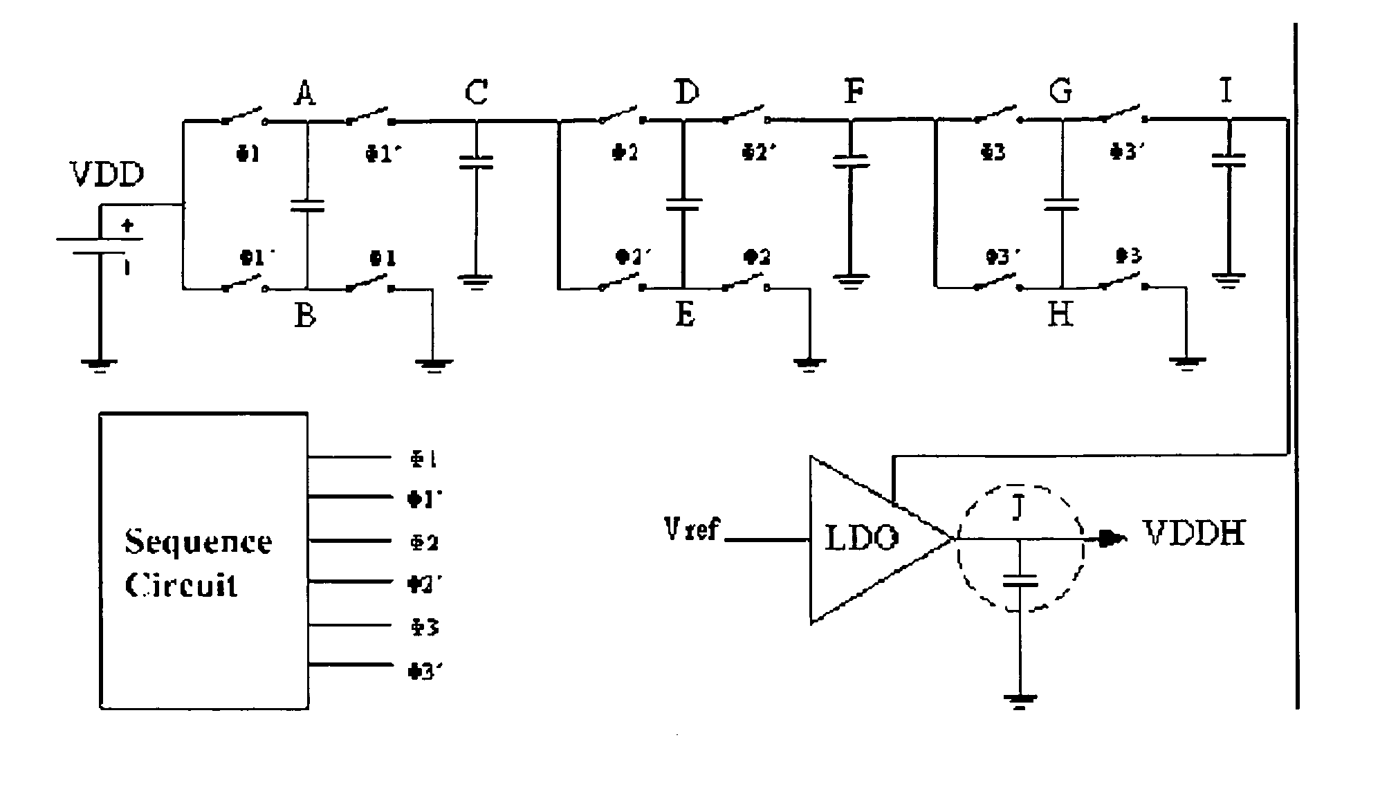
[0034]FIG. 5 illustrates a boost circuit of a capacitive touch panel detection circuit according to a first preferred embodiment of the invention. The boost circuit adopts a charge pump (a switched capacitor voltage converter) to replace the inductive boost circuit in FIG. 2. It has the advantages that: the capacitor in the invention can be integrated into the inner part of a chip, while the inductor in FIG. 3 can not be integrated or the process cost is high; a Schottky diode with high voltage and high power is also difficult to be integrated into the inner part of the chip. A typical embodiment of an eight-time charge pump is shown in FIG. 4. It mainly comprises a sequence circuit, a switch (MOS transistor), a capacitor and a LDO linear regulator. For the capacitor part, except a voltage-stabilizing capacitor J of VDDH in a dashed frame, others are all internal capacitors. It is a three-stage boost circuit with the voltage increased by two times each stage under the ideal conditio...


PUM


Abstract

The invention discloses a capacitive touch panel detection circuit and a boost circuit thereof, wherein the boost circuit comprises a plurality of charge pumps in series, a sequence circuit and a voltage-stabilizing circuit. The charge pump comprises a first switch, a second switch, a third switch, a fourth switch, a first capacitor and a second capacitor. The switches are controlled by the sequence circuit. During the first half of the working cycle of the charge pump, the first capacitor is charged. During the second half of the working cycle of the charge pump, the second capacitor is charged so that the voltage is two times of the power voltage, after the first capacitor is connected with the power supply in sequence. The boost circuit of the invention does not need an induction and a Schottky diode. All of the capacitors except a voltage-stabilizing capacitor can be integrated into a chip. Therefore, the number of off-chip ancillary components can be reduced. Furthermore, the problem of electromagnetic interference in an inductive boost circuit can be solved.

Description

BACKGROUND OF THE PRESENT INVENTION[0001]1. Field of Invention[0002]The invention relates to a touch technique, in particular to a capacitive touch panel detection circuit and a boost circuit thereof.[0003]2. Description of Related Arts[0004]In the 1970s, U.S. Military firstly utilized the technique of touch panel in the military field. Since then, this technique has been gradually turned to the civilian field. With the development of network techniques and the popularization of the internet, people successively witnessed the emerging of the new generation of the touch technique and products which attract the users with their advantages of hardness and durability, rapid response, space saving and easy communication. At present, these relaxing human-computer interaction techniques have be used in many other fields. Except the field of personal portable information products (such as the handwriting input technique of PC, PDA, AV and so on), these techniques have been used in the field...

Claims


Application Information

Patent Timeline
IPC IPC(8): H03K17/96G05F3/02
CPCH02M3/07G06F3/044G06F3/0416G06F3/04166
Inventor MO, LIANGHUALIU, WENPING
Owner FOCALTECH ELECTRONICS SHENZHEN CO LTD
Why Eureka
Try Eureka