Layering placement modeling method for modern programmable logic device software system

A technology of software system and modeling method, which is applied in the electronic field and can solve problems such as unusable

Inactive Publication Date: 2008-07-30
FUDAN UNIV
View PDF0 Cites 18 Cited by
  • Summary
  • Abstract
  • Description
  • Claims
  • Application Information

AI Technical Summary

Problems solved by technology

thus making the method unusable in industry

Method used


Image

  • Layering placement modeling method for modern programmable logic device software system
  • Layering placement modeling method for modern programmable logic device software system
  • Layering placement modeling method for modern programmable logic device software system

Examples


Embodiment Construction

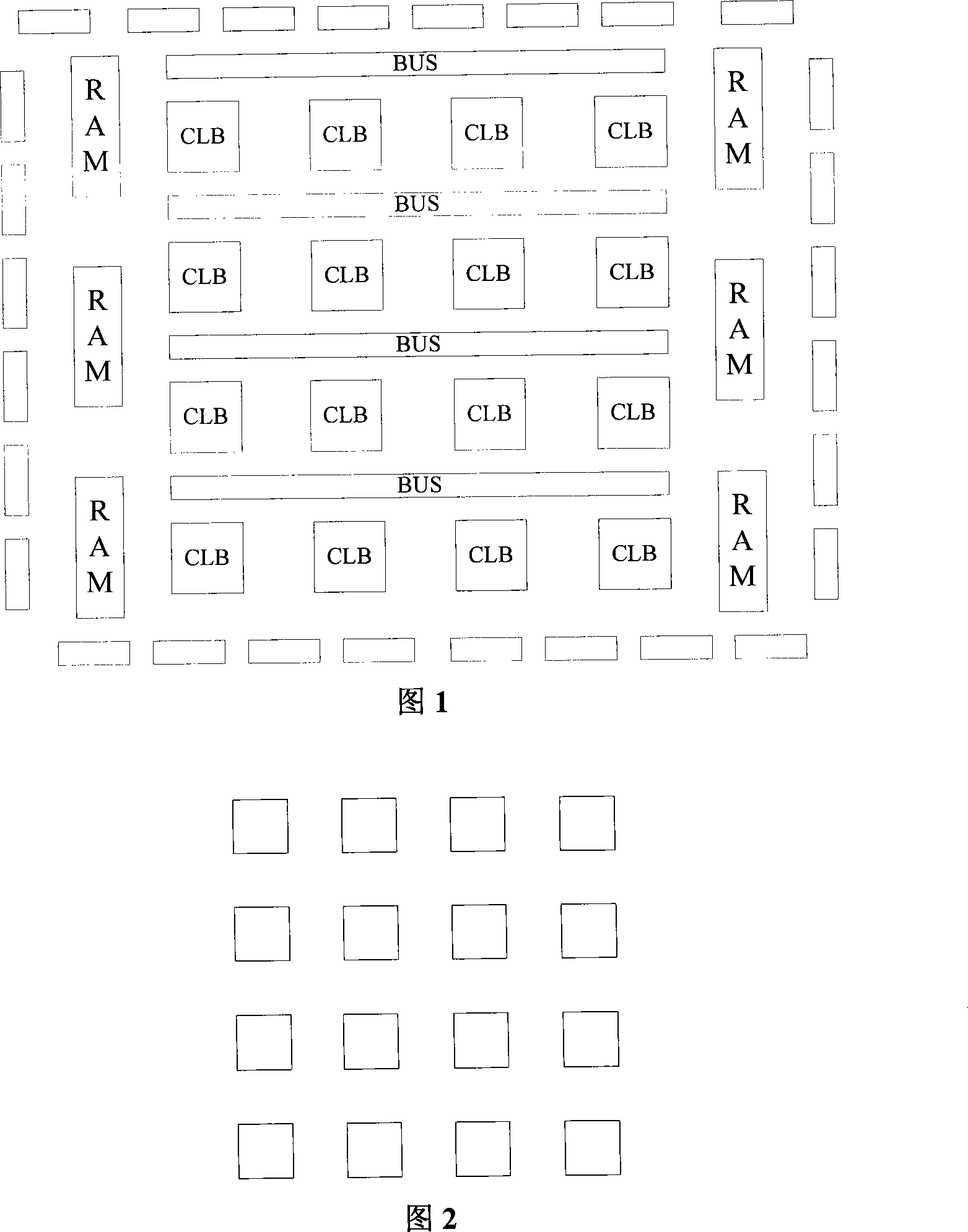
[0023] Taking the SpartanII chip of Xilinx Company as an example, its chip structure is shown in Figure 1. The chip has a total of programmable logic block (SLICE), programmable input and output block (IOB), bus (TBUF), block random access memory (RAM) and other module types. The programmable logic block (SLICE) is evenly distributed within the chip area; the bus (TBUF) is distributed between each row of programmable logic blocks (SLICE); the block random access memory (RAM) is distributed on the left and right sides of the chip area; programmable Input-output blocks (IOBs) are distributed around the chip area.

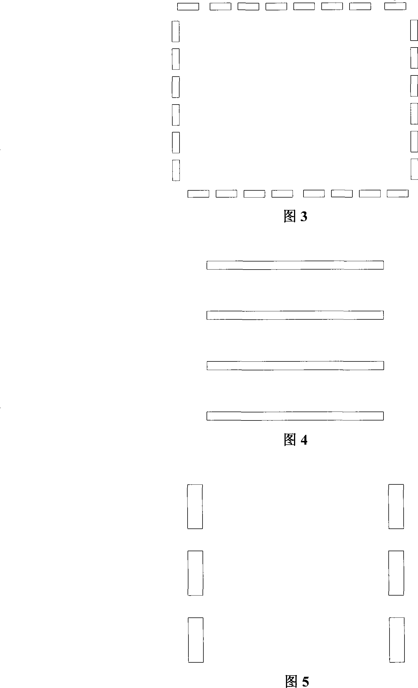
[0024] All logic units of the same type on the FPGA chip form a logic unit layer. The structure of the programmable logic block (SLICE) layer is shown in Figure 2; the structure of the programmable input-output block (IOB) layer is shown in Figure 3; the structure of the bus (TBUF) logic layer is shown in Figure 4; block random access memory (RAM) The structure of t...


PUM


Abstract

The invention belongs to the electronic technology field, in particular to a hierarchical layout design modeling method of a modern FPGA software system. The invention is a layout software modeling method aiming at a modern FPGA hardware structure, and has the details that the FPGA structure is logically divided into a plurality of logic unit layers according to the types of the logic unit, such as a programmable logic block layer, a programmable input-output block layer, a block random memory layer, a bus layer and a global clock layer, etc.; then models are respectively established on each logic unit layer according to a specific geometric structure, and the layout scheme is adjusted according to the practical situation. The invention can greatly improve the running efficiency and the algorithm expansibility of the FPGA layout software in the whole FPGA CAD process through respectively carrying out the layout on each logic unit layer.

Description

technical field [0001] The invention belongs to the field of electronic technology, and in particular relates to a software modeling method of a programmable logic device (FPGA) structure. technical background [0002] An efficient CAD system is a necessary condition for using FPGA. Modern FPGAs have diverse and complex logic and resources. Taking Xilinx's Spartan II chip as an example, in addition to programmable logic blocks and programmable input and output blocks, there are also various logic resource types such as random access memory, buses, and global clocks. At present, the classic layout software VPR commonly used in academia is aimed at a very simple structure, with few wiring resources, and almost no dedicated logic or dedicated wiring. It is not suitable for logic resources such as macros, buses, and multiple clocks that often appear in modern FPGA structures. support. Although generally speaking, the structure and algorithm targeted by VPR are in an important ...

Claims


Application Information

Patent Timeline
Patent Type & Authority Applications(China)
IPC IPC(8): G06F17/50
Inventor 来金梅徐嘉伟扬铭童家榕
Owner FUDAN UNIV
Why Eureka
Try Eureka