Electronic component transfer loading device and method

A technology of electronic components and transfer devices, which is applied in the direction of measuring devices, electronic circuit testing, measuring electricity, etc., can solve the problems of increasing production costs, affecting test quality, poor level, etc.

Active Publication Date: 2008-08-06
HON PRECISION INC
View PDF1 Cites 23 Cited by
  • Summary
  • Abstract
  • Description
  • Claims
  • Application Information

AI Technical Summary

Problems solved by technology

[0003] Because the reclaimers 25 and 35 of the first and second reclaiming mechanisms 20 and 30 with suction nozzles can only be displaced in the X-Z two axial directions, the reclaimers 25 and 35 cannot be placed at each pick-and-place position and test position. Fine-tuning the X-Y-Z three-axis position, so the displacement positioning position of the carrier 41, 51 relative to the test platform 10, and the displacement positioning position of the reclaimer 25, 35 relative to the test platform 10, the carrier 41, 51, in the assembly The design must have absolute precision so that the reclaimers 25 and 35 can accurately carry the IC for testing under the displacement limit of the X-Z two axes. Such high-precision production requirements make the production difficult and greatly The problem of increasing production costs
In addition, the reclaimers 25, 35 are mounted on both sides of the test bench 10 in the form of L-shaped cantilevers, and the suction nozzles 253, 353 are pressed against the IC to be tested, which may cause poor levelness and affect the test. quality

Method used


Image

  • Electronic component transfer loading device and method
  • Electronic component transfer loading device and method
  • Electronic component transfer loading device and method

Examples


Embodiment Construction

[0026] The above and other technical features and advantages of the present invention will be described in more detail below in conjunction with the accompanying drawings.

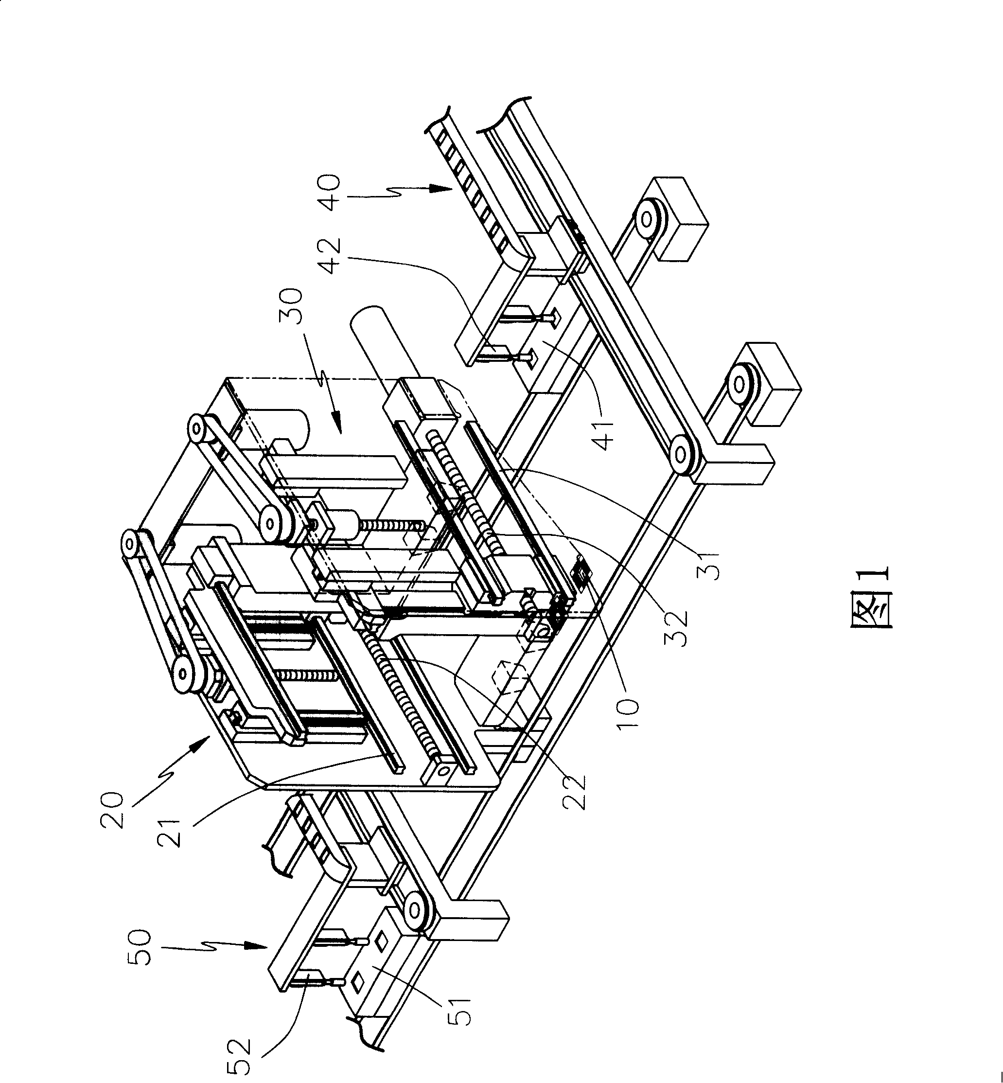
[0027] Please refer to Fig. 4, when the present invention is configured in a test classifier, the test classifier includes a feeding mechanism 60, an input conveying mechanism 70, a work station area 80, an output conveying mechanism 90 and a receiving mechanism 100 The input end conveying mechanism 70 is to transport the electronic components to be detected on the feeding mechanism 60 to the first and second feeding carriers 81, 82 in the operation area 80 respectively, and the first and second receiving carriers in the operation area 80 The tested electronic components on the material carriers 83 and 84 are transported by the output conveying mechanism 90 to the receiving mechanism 100 for sorting and placing according to the test results.

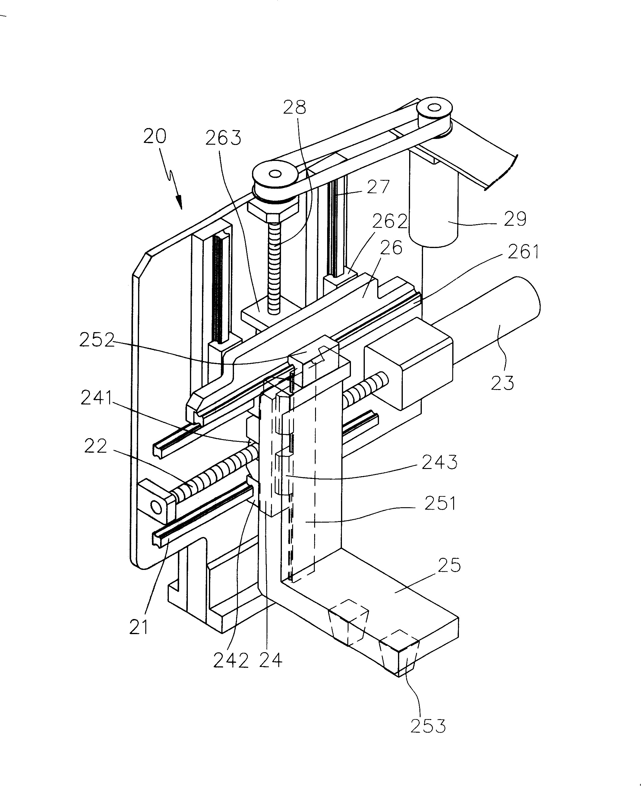
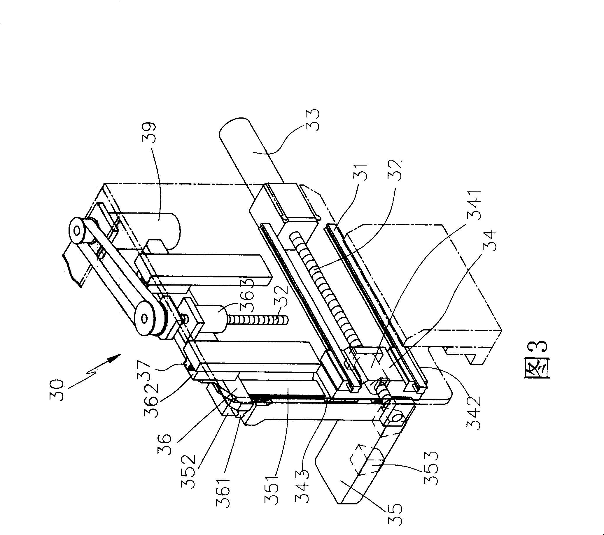
[0028]Referring to Fig. 5 and Fig. 6, the operation area 80 of ...


PUM


Abstract

The invention relates to an electronic component transferring device and a method, comprising at least a work station for the transferring of the electronic device to work and executing work, a first feeding carrier arranged on a side of the work station to bear the electronic device to work, a second feeding carrier arranged on another side of the work station to bear the electronic device to work, a first material receiving carrier arranged on the same side with the first feeding carrier to bear the electronic device finishing work, a second material receiving carrier arranged on the same side with the second feeding carrier to bear the electronic device finishing work, a first transferring taking and placing device arranged on a chassis above the work station through a slide group frame to slide in three axial directions and transfer the electronic device for executing work, and a second transferring taking and placing device arranged on the chassis above the work station through the slide group frame to slide in three axial directions and transfer the electronic device for executing work. Therefore, the invention achieves the purpose of stably transferring the electronic device into the work station for executing work, facilitating the manufacture, and easily improving the work quality.

Description

technical field [0001] The present invention relates to a carrying device and method, in particular to a first transfer pick-and-place device and a second transfer pick-and-place device which are installed above the work station and can perform three-axis sliding movements. The device is used to alternately transfer the electronic components to the work station, and put the electronic components into the work station at a stable level to perform operations, so as to achieve an electronic component transfer device and method that is easy to manufacture and improves the quality of work. Background technique [0002] Please refer to Figure 1, figure 2 , Fig. 3, it is Taiwan patent application No. 93110783 " IC detection device (two) " patent case, described detection device comprises test bench 10, the first, the second feeding mechanism 20,30 and the feeding and discharging mechanism 40,50, wherein, the two sides of the test bench 10 are provided with first and second materia...

Claims


Application Information

Patent Timeline
Patent Type & Authority Applications(China)
IPC IPC(8): B65G37/00B65G47/91G01N35/02G01R31/28H01L21/66
CPCG01R31/2831
Inventor 张简荣力
Owner HON PRECISION INC
Why Eureka
Try Eureka