

Output adjustable band-gap reference source circuit
A reference source circuit, adjustable technology, applied in the direction of adjusting electrical variables, control/regulating systems, instruments, etc., can solve problems such as difficult current replication
Inactive Publication Date: 2010-08-18
INST OF SEMICONDUCTORS - CHINESE ACAD OF SCI
View PDF0 Cites 1 Cited by
- Summary
- Abstract
- Description
- Claims
- Application Information
AI Technical Summary
Problems solved by technology
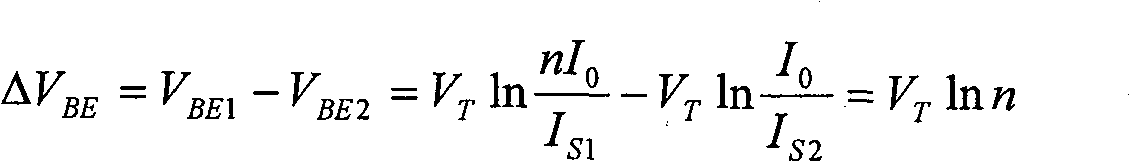
However, it can be seen from the following voltage-current conversion circuit that the voltage 1.22V generated by this structure is too high compared to the power supply voltage of 3.3V, and it is difficult to accurately replicate the current generated by using the cascode structure to the Post-stage use
Method used
View moreImage
Smart ImageViewing Examples

Examples
Embodiment Construction
Login to View More PUM
 Abstract
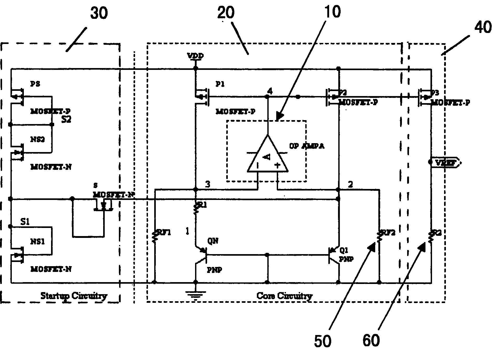
An output adjustable band-gap reference source circuit is characterized by comprising: a high-gain operational amplification circuit; a voltage generation circuit independent of temperature and power source connected with the input end and output end of the high-gain operational amplification circuit by nodes, so as to implement output clamping effect; a start circuit, the output of which is connected to the node of the voltage generation circuit independent of temperature and power source to prevent the voltage generation circuit independent of temperature and power source entering a dead region; an output regulation circuit, the input of which is connected to the voltage generation circuit independent of temperature and power source, thereby to implement output clamping effect, and the output is the output of the whole band-gap reference source circuit.
Description
technical field The invention relates to the technical field of a reference source (Bandgap) circuit, in particular to a reference source (Bandgap) circuit for providing a variable output voltage. Background technique The reference voltage source is an important unit module in an integrated circuit, and is a basic element in an analog-to-digital converter (ADC) and a digital-to-analog converter (DAC) as well as a communication circuit. Its temperature stability and anti-noise ability are key factors affecting the conversion accuracy of analog-to-digital converters (ADC) and digital-to-analog converters (DAC), and even affect the accuracy and performance of the entire system. Therefore, designing a good reference voltage source has very important practical significance. The bandgap reference source circuit has been widely researched and applied because of its low temperature coefficient, low power supply voltage and compatibility with standard CMOS processes. Its principle ...
Claims
Login to View More Application Information
Patent Timeline
 Patent Type & AuthorityPatents(China)
IPC IPC(8): G05F3/08G05F3/20
Inventor倪卫宁石寅
OwnerINST OF SEMICONDUCTORS - CHINESE ACAD OF SCI