Method for manufacturing multilayer printed wiring board

A technology of multi-layer printing and manufacturing method, applied in the direction of multi-layer circuit manufacturing, printed circuit manufacturing, printed circuit, etc., can solve the problems of reduced quality, complicated manufacturing process, damage of insulating resin layer, etc., to improve bending resistance and reliability. high sex effect

Inactive Publication Date: 2008-09-03
SHARP KK
View PDF19 Cites 7 Cited by
  • Summary
  • Abstract
  • Description
  • Claims
  • Application Information

AI Technical Summary

Problems solved by technology

[0005] In addition, since the mounting portion for mounting the electronic components has at least a certain degree of rigidity for mounting the electronic components and mounting to the housing, compared to the cable portion that requires flexibility, it is easy to handle, so it must be formed while having Flexible and rigid multilayer printed wiring boards have problems such as complicated manufacturing processes and deformation at the boundary between the flexible part and the rigid part.
Therefore, there is a problem that the interlayer adhesive flows in the direction of the flexible part where the gap occurs, and the layer thickness of the multilayer part near the flexible part (boundary position BP) gradually becomes thinner, or the interlayer adhesive Spills to create unwanted bonding on the flex so that the outer substrate on the flex cannot be peeled off
[0052] In addition, the base material cannot be peeled even if it does not reach the outer layer, but there is a problem that the quality of the interlayer adhesive is degraded due to the outflow of the interlayer adhesive in the vicinity of the boundary position BP.
Another problem is that when stacking, the edge of the window portion (hole or slit) is affected by the blade, which damages the flexible portion at the boundary position between the flexible portion and the multi-layer portion, and makes many of the finished state The bending performance of the flexible part in the multi-layer printed wiring board, especially the double-folding property of the flexible part at the boundary position BP is reduced
[0053] (2) If the outer base material is subjected to slit processing in advance to remove the outer base material on the flexible part in advance, there will be a problem that, in the decontamination process when the through hole or auxiliary hole is formed, the The inner layer base material or the insulating resin layer of the flexible part in the exposed state of the layer removal part (window part) is damaged, and the insulation properties, interlayer adhesive strength, bending resistance, friction resistance, etc. are significantly reduced
In addition, there is a problem that not only in the decontamination process, but also in the pretreatment (such as grinding, surface treatment) of each processing step, it is damaged, or conversely, around the boundary position BP, due to the difference in height, the processing is not smooth. full
However, there is a problem that when the surface treatment (such as electroplating) is performed on the terminal part, it will be peeled off in the subsequent grinding process. In addition, in the case of a copper foil substrate, it will be etched when the outer layer pattern is etched. , must somehow cover the flexible part, at least the terminal part
[0056] Due to such a problem, the actual problem is that there is no terminal in the flexible part, and it can only be used in the case of a form (folding type, see FIG. 10 ) that connects a plurality of multilayer parts with a flexible part

Method used


Image

  • Method for manufacturing multilayer printed wiring board
  • Method for manufacturing multilayer printed wiring board
  • Method for manufacturing multilayer printed wiring board

Examples


Embodiment Construction

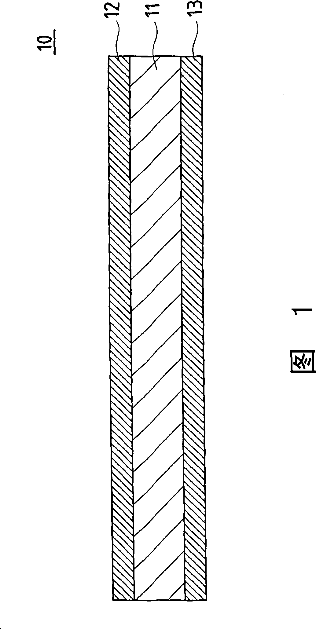
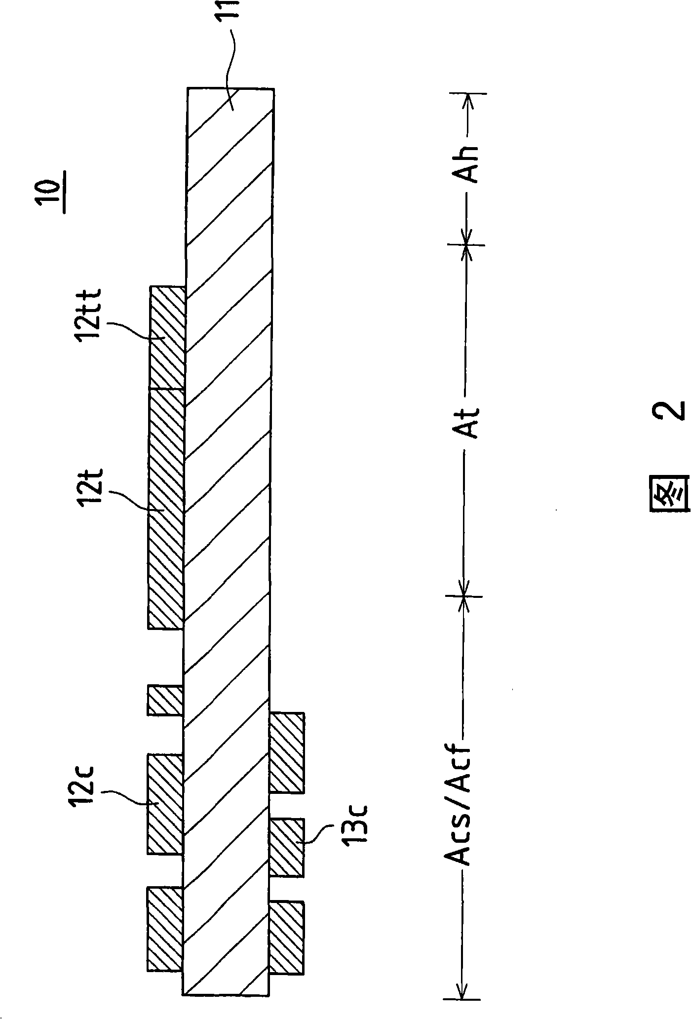
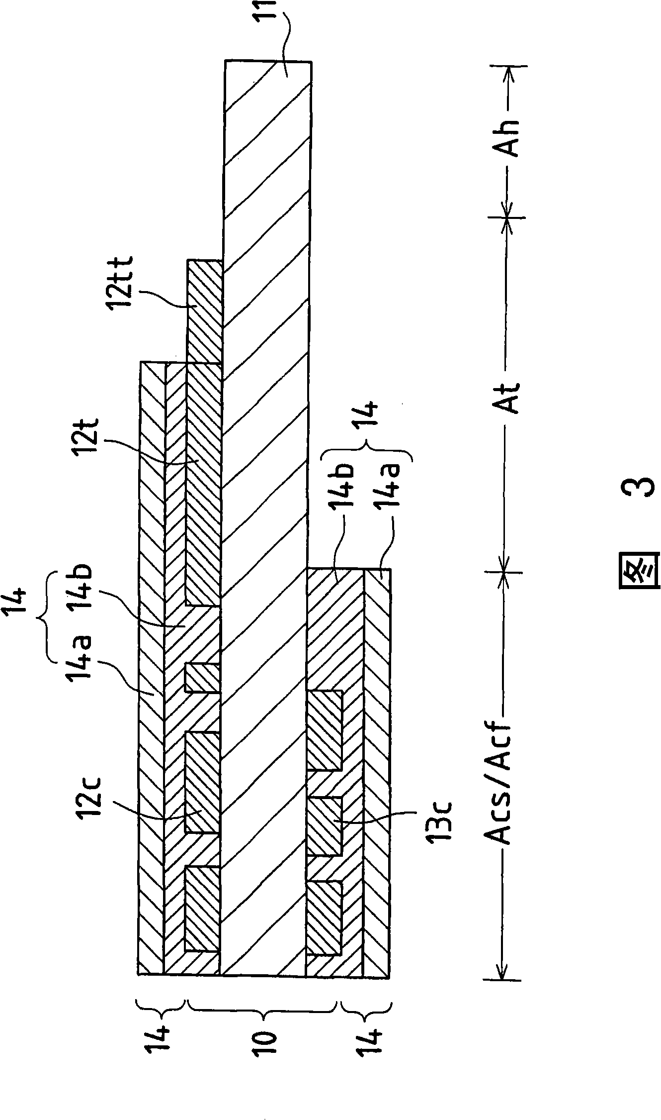
[0094] Hereinafter, embodiments of the present invention will be described with reference to the drawings. In addition, in the embodiments described below, in order to simplify the description, a multilayer printed wiring circuit composed of a flexible part (lead pattern part) as one conductor layer and a multilayer part (laminated circuit pattern part) as four conductor layers The board is described as an example, but the laminated circuit pattern part is not limited to four conductor layers, and may have three conductor layers or other multilayer structures. In addition, it can be applied to multilayer printed wiring boards of all forms represented by common name build-up boards such as laser method / optical via method.

[0095]

[0096] A method of manufacturing the multilayer printed wiring board according to the first embodiment will be described with reference to FIGS. 1 to 9 .

[0097] In the first embodiment, a multilayer printed wiring board in which a flexible lead...


PUM


Abstract

In one embodiment, an inner layer pattern formation step of patterning a conductor layer of an inner layer base material to form an inner layer circuit pattern of an inner layer circuit pattern portion and a lead pattern of a lead pattern portion, a resin film affixing step of affixing a resin film to the lead pattern portion, an outer layer base material layering step of layering / fastening to the inner layer base material an outer layer adhesive layer disposed corresponding to the inner layer circuit pattern portion and an outer layer conductor layer disposed corresponding to the inner layer base material, an outer layer pattern formation step of patterning the outer layer conductor layer to form an outer layer circuit pattern portion corresponding to the inner layer circuit pattern portion, and a resin film peeling step of peeling away the resin film from the lead pattern portion, are provided.

Description

[0001] This application claims priority based on Japanese Patent Application No. 2007-049898 filed in Japan on February 28, 2007. Accordingly, the entire content thereof is included in this application. technical field [0002] The present invention relates to a method for manufacturing a multilayer printed wiring board, which is used in electronic equipment and the like, and includes: a flexible inner layer base material having an inner layer circuit pattern portion and a lead pattern portion; The outer layer base material of the outer layer circuit pattern part on which the inner layer circuit pattern part is laminated. Background technique [0003] In portable electronic devices such as video cameras and digital cameras, many electronic components must be arranged in a small internal space and connected with each other by wiring. [0004] In the past, connectors and cables were used to connect hard printed wiring boards to each other, but for the purpose of connection re...

Claims


Application Information

Patent Timeline
Patent Type & Authority Applications(China)
IPC IPC(8): H05K3/46
CPCH05K3/046H05K3/243H05K3/281H05K3/4652H05K3/4691H05K2201/0195H05K2203/0191
Inventor 上野幸宏冈田宏明
Owner SHARP KK
Why Eureka
Try Eureka