A method for making horizontal dual pervasion field effect transistor

A field effect transistor, lateral double diffusion technology, applied in semiconductor/solid state device manufacturing, electrical components, circuits, etc., can solve problems such as increasing costs, and achieve the effect of expanding capacity and reducing costs

Active Publication Date: 2008-09-17
SEMICONDUCTOR MANUFACTURING INTERNATIONAL (BEIJING) CORP +1
View PDF0 Cites 32 Cited by
  • Summary
  • Abstract
  • Description
  • Claims
  • Application Information

AI Technical Summary

Problems solved by technology

However, these methods need to introduce some special steps, such as the...

Method used


Image

  • A method for making horizontal dual pervasion field effect transistor
  • A method for making horizontal dual pervasion field effect transistor
  • A method for making horizontal dual pervasion field effect transistor

Examples


Embodiment Construction

[0023] The present invention will be described in further detail below in conjunction with the specific implementation manner of accompanying drawing and N-type LDMOS device:

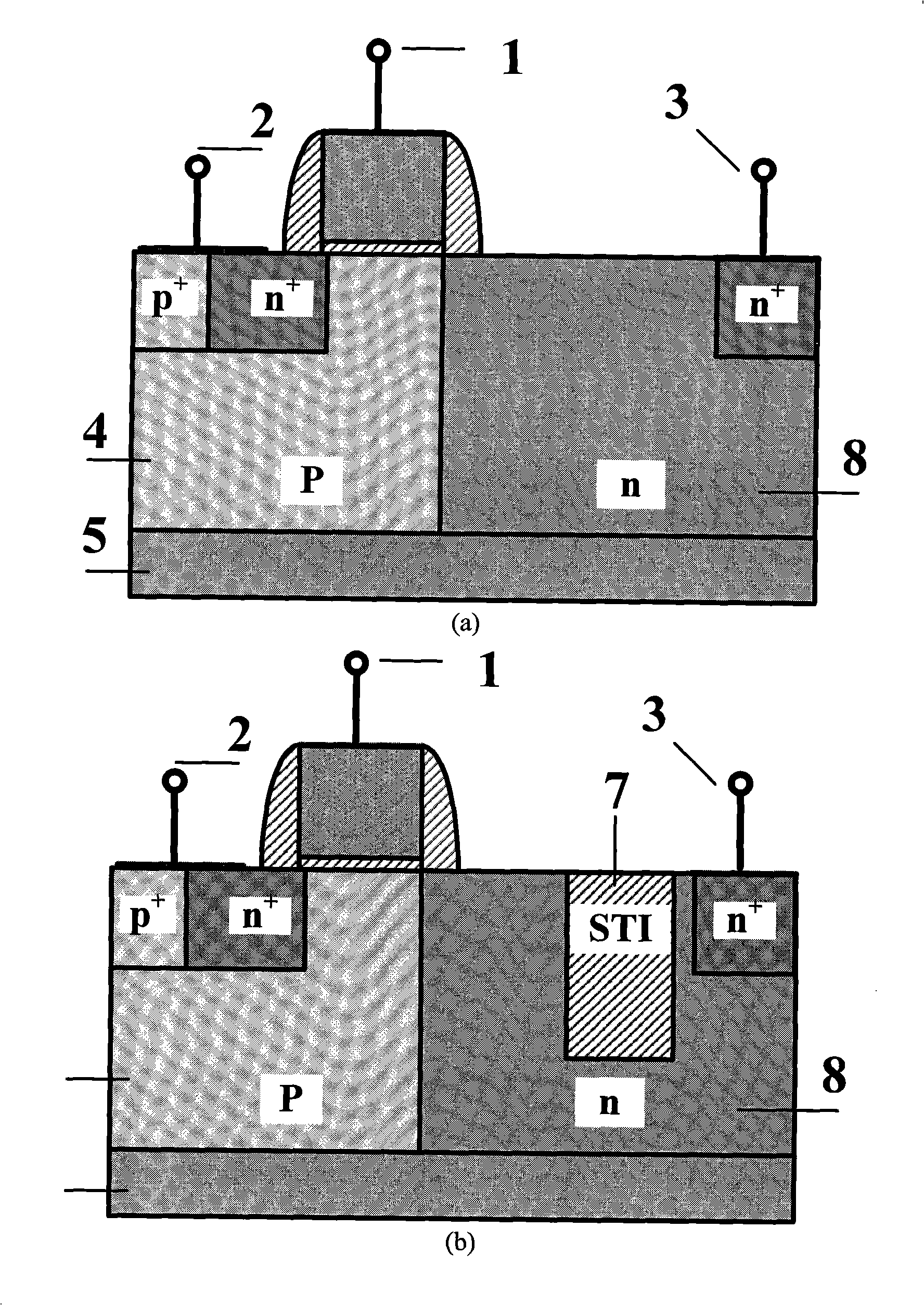
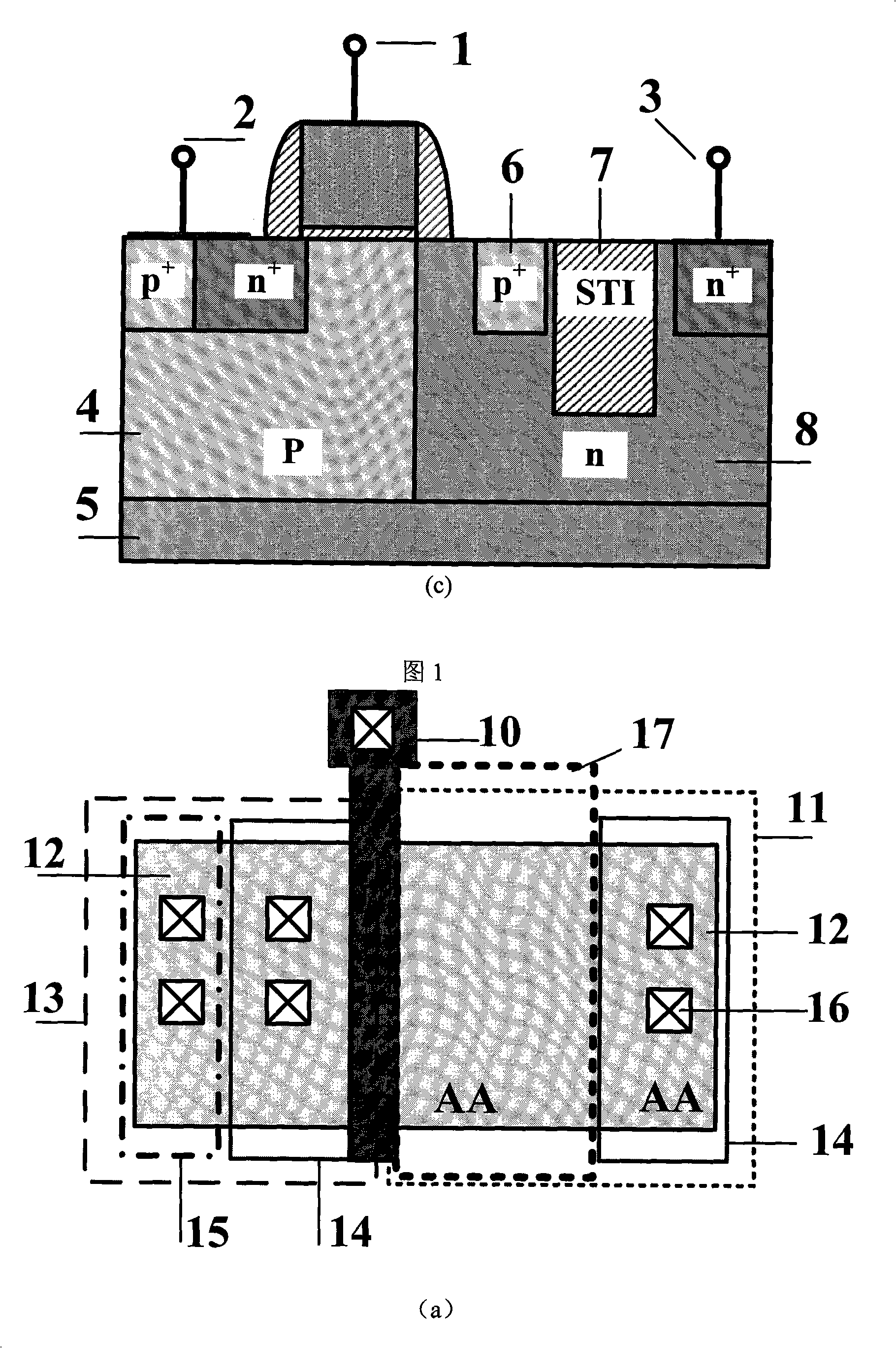
[0024] Figure 1 shows three LDMOS structures prepared by this method. The main difference between LDMOS and conventional MOS field effect transistors is that there is a low-doped drift region (Figure 1(a)). The drift region of LDMOS can be further optimized by introducing a doped implant region or an insulating impurity region, as shown in Figure 1(b) and Figure 1(c). However, the LDMOS structure shown in Fig. 1 can be realized only by using the standard CMOS process through the method of layout design.

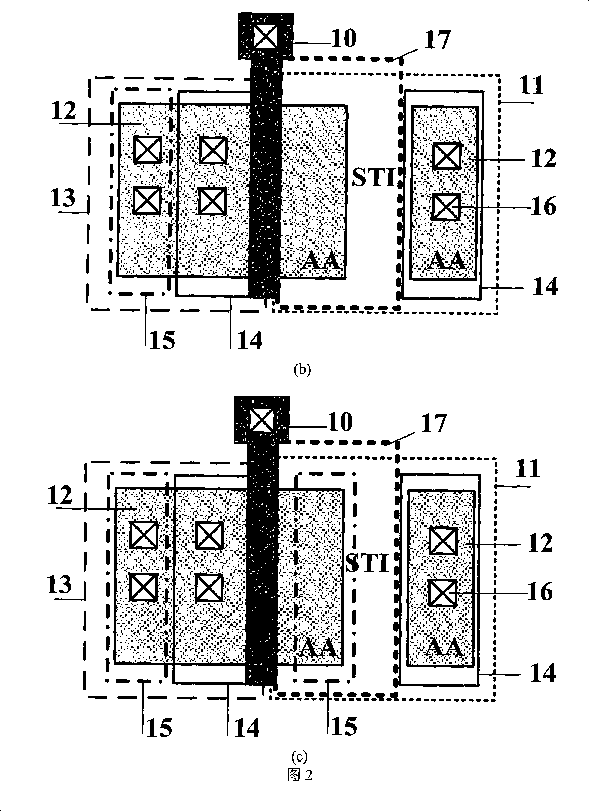
[0025] Figure 2 shows a schematic diagram of the layout design for preparing the structure shown in Figure 1(c). In the figure: the layout of the N well is used in the layout to form the low-doped drift region of the N-type LDMOS, the layout of the P well forms the body region, and the body lead-out ...


PUM

PropertyMeasurementUnit
Lengthaaaaaaaaaa
Horizontal lengthaaaaaaaaaa

Abstract

The invention discloses a method for manufacturing a laterally dual-diffused FET (field effect transistor), belonging to FET manufacturing field, the method is achieved by using the method for manufacturing LDMOS according to standard CMOS manufacturing processes, to realize LDMOS via chart design as following: defining a active layout to form a body extracting area, a source area, a drain area, a channel area, a drift area and a grid area of a LDMOS element; the source area, grid area and drain area are formed according to a re-doping injection layout; the drift area is disposed between the drain area and the channel area; both of the body extracting area and the source area are in grounding connection; using a N well layout to form a low-doping drift area of a N type LDMOS, or using P well layout to form a P type low-doping drift are of a P type LDMOS; using anti-silicification board to prevent the drift area from being silicified; the design of the source area, the drain area and the grid area complies with the normal MOS. The invention can be applied on any standard process, effectively reducing costs, and improving the capability of standard process for manufacturing special elements.

Description

technical field [0001] The invention relates to a preparation method of a field effect transistor, in particular to a preparation method of a lateral double-diffusion field effect transistor. Background technique [0002] A lateral double-diffused MOS transistor (lateral double-diffused MOS transistor, LDMOS) is a lightly doped drain MOS device. Compared with ordinary MOS devices, LDMOS has a longer lightly doped implantation region at the drain end, usually the doping concentration of this part of the structure is 10 16 cm -3 magnitude, known as the drift region. The LDMOS structure withstands a higher voltage drop through the drift region. Because LDMOS technology is simple, reliable, mature, and has good RF performance, and because the manufacturing process of LDMOS transistors is fully compatible with existing standard CMOS processes, it is easier to achieve large-scale integration with low-voltage CMOS circuits and reduce manufacturing cost. It is mainly used in va...

Claims


Application Information

Patent Timeline
IPC IPC(8): H01L21/336
Inventor 肖韩黄如王鹏飞杨淮洲
Owner SEMICONDUCTOR MANUFACTURING INTERNATIONAL (BEIJING) CORP
Why Eureka
Try Eureka