Optical waveguide device and manufacturing method for the same

A manufacturing method and technology of optical waveguides, which are applied in the directions of optical waveguides, optical waveguides, coupling of optical waveguides, and optical waveguides, can solve problems such as inability to identify, technology is not effective, and difficult, and achieve the effect of improving installation accuracy and productivity.

Inactive Publication Date: 2008-09-24
NEC CORP
View PDF1 Cites 27 Cited by
  • Summary
  • Abstract
  • Description
  • Claims
  • Application Information

AI Technical Summary

Problems solved by technology

Performing this adjustment is very difficult for 1D linear alignment marks
For example, if the optical axis of the optical waveguide is misaligned by 1-2 degrees, then a big problem occurs, however, such small misalignments cannot practically be identified with alignment marks that are much shorter than the length of the optical waveguide
Also, because the image needs to be within the screen of the monitor used for alignment, the length of the alignment marks cannot extend
Therefore, these techniques are not effective in any alignment other than 1D

Method used


Image

  • Optical waveguide device and manufacturing method for the same
  • Optical waveguide device and manufacturing method for the same
  • Optical waveguide device and manufacturing method for the same

Examples


Embodiment Construction

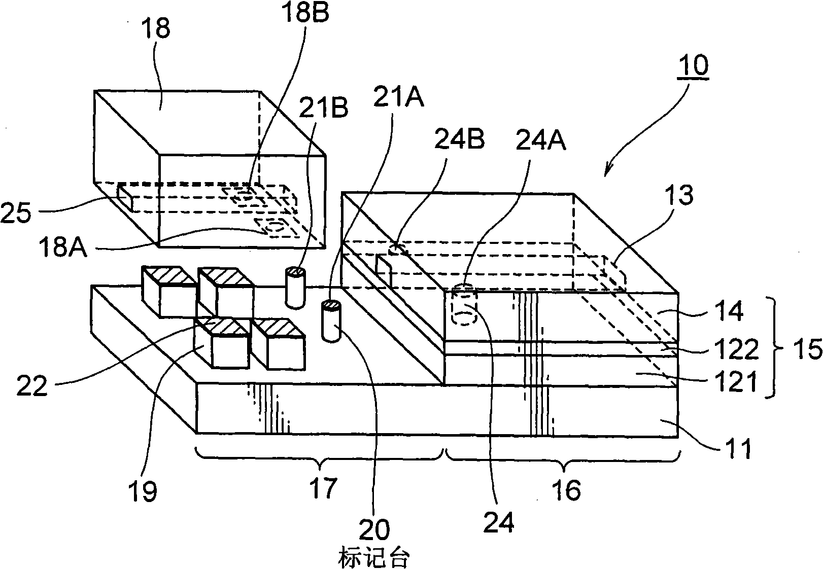
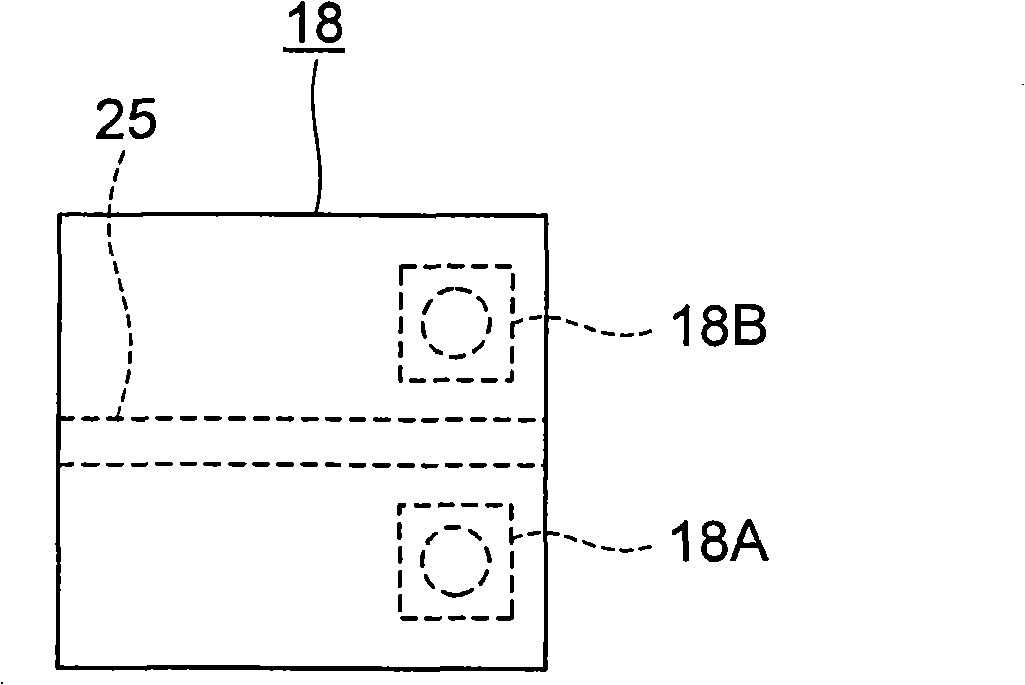
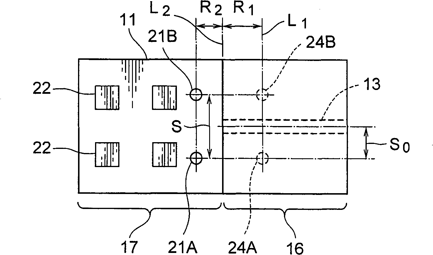
[0039] Hereinafter, an exemplary embodiment of the present invention will be described with reference to the drawings. figure 1 A conceptually exploded perspective view of an optical waveguide device according to an exemplary embodiment is shown. Figure 2A and 2B A plan view of the optical waveguide device is shown. exist figure 1 Among them, the optical waveguide device 10 includes a substrate 11 made of silicon crystal, an optical waveguide forming portion 16 provided on a portion of the substrate 11, an optical device mounting portion 17 (optical device mounting area) provided on the other portion of the substrate 11 , corresponding to the optical waveguide forming portion 16. The optical waveguide forming portion 16 includes the optical waveguide portion 15 formed with the base layer 121, the lower cladding layer 122, the optical waveguide core 13, and the upper cladding layer 14 laminated on the substrate 11, all of which are made of CVD films.

[0040] Regarding t...


PUM


Abstract

To obtain an optical waveguide device capable of improving mounting accuracy and productivity for correcting misalignment of alignment marker caused by distortion due to a substrate stressed and distorted. An optical waveguide device includes an optical waveguide section, including a waveguide core formed on a substrate, and an optical device (LD) mounted on the substrate to correspond the optical waveguide section, both of which are coupled at a light end face and mounted by hybrid mounting. LD side alignment markers are provided in both sides of an active line in the optical device. Substrate side alignment markers are provided at positions where centers thereof and those of the optical device side markers are matched when the optical device is mounted on the corresponding substrate. Fiducial markers are formed during the formation of the core so that the relative positional relationship with the waveguide core on the substrate becomes stable. Thus, a misalignment amount is detected.

Description

[0001] Cross References to Related Applications [0002] This application is based on and claims the benefit of priority from Japanese Patent Application No. 2007-077566 filed on March 23, 2007, the disclosure of which is incorporated herein by reference in its entirety. technical field [0003] The present invention relates to an optical waveguide device and the like, and more particularly, to an optical waveguide device and a method of manufacturing the same for improving accuracy and productivity when mounting an optical device on a corresponding position of an optical waveguide. Background technique [0004] Optical transceivers used in the optical access market include micro-optical modules composed of LDs, PDs, thin film filters, lenses, etc. and PLC modules composed of silica waveguides formed on silicon substrates, mounted on LDs and PDs are also mounted on the silicon substrate. Both have advantages and disadvantages. In terms of cost and delivery, the latter is ...

Claims


Application Information

Patent Timeline
Patent Type & Authority Applications(China)
IPC IPC(8): G02B6/122G02B6/42G02B6/13
CPCG02B6/42G02B6/4227G02B6/4224G02B6/12
Inventor 渡边真也栗原充
Owner NEC CORP
Why Eureka
Try Eureka