Board structure and electronic device

A technology for electronic equipment and substrates, applied in the direction of electrical equipment structural parts, circuits, printed circuits, etc., can solve the problems of lack of shielding, structural barriers, and insufficient mounting strength of electronic component substrates, so as to ensure the mounting strength. Effect

Inactive Publication Date: 2008-09-24
PANASONIC CORP
View PDF1 Cites 14 Cited by
  • Summary
  • Abstract
  • Description
  • Claims
  • Application Information

AI Technical Summary

Problems solved by technology

[0009] However, the above-mentioned Patent Document 1 has a problem that sufficient shielding properties cannot be obtained because a plurality of notches are provided in the reinforcing frame.
[0010] In addition, the above-mentioned Patent Document 1 also has the following problem: the resin is filled from the gap in the reinforcement frame to the inside, but the reinforcement frame becomes an obstacle, so the electronic components can only be reinforced to the degree of underfullness, and the electronic components are relatively weak. The mounting strength of the substrate may not be sufficient

Method used


Image

  • Board structure and electronic device
  • Board structure and electronic device
  • Board structure and electronic device

Examples


no. 2 Embodiment approach

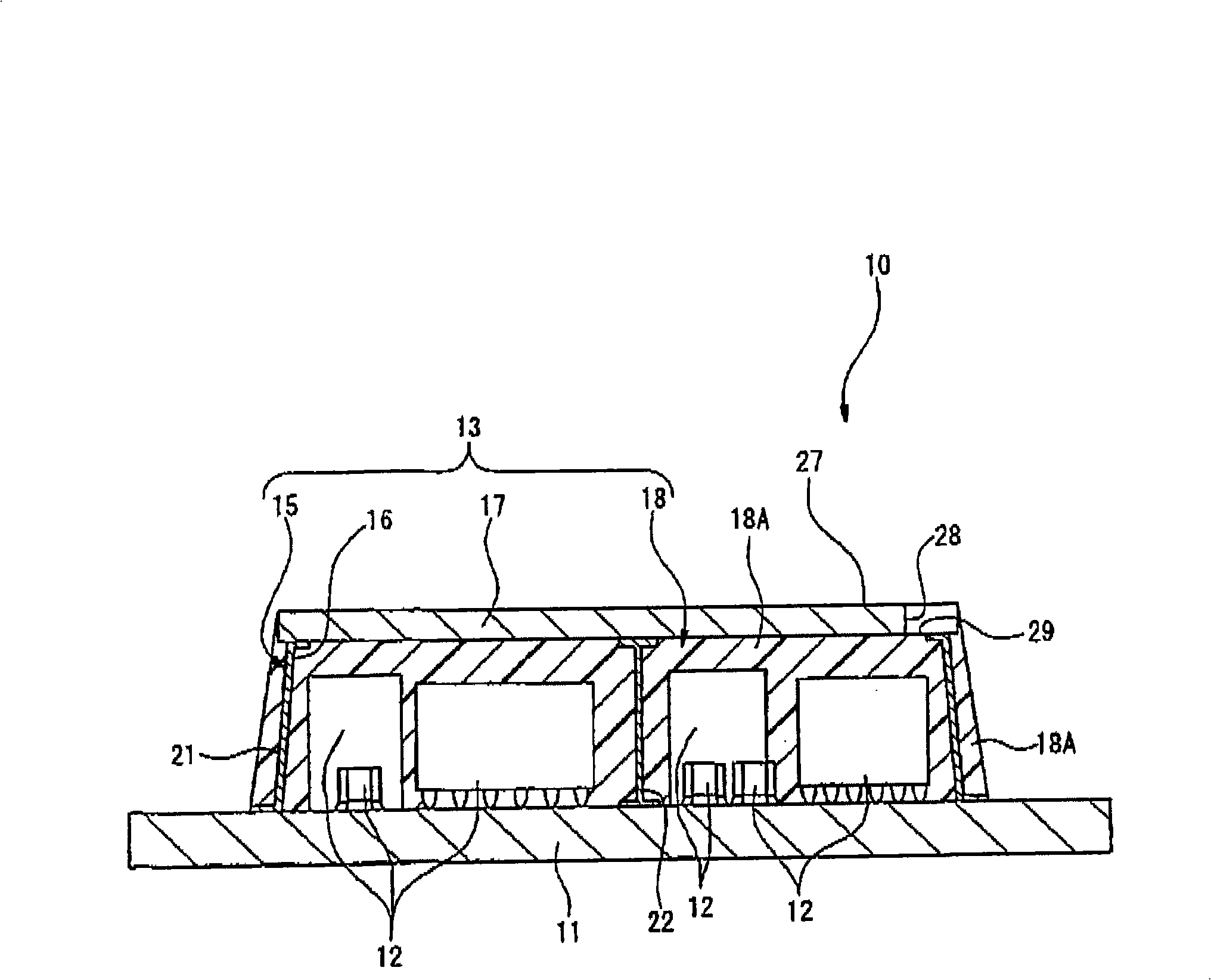
[0084] The substrate structure 40 of the second embodiment shown in FIG. 5 is a structure in which the resin 18 of the first embodiment is replaced with a resin 41 , and the other configurations are the same as those of the substrate structure 10 of the first embodiment.

[0085] The resin 41 is a resin that is injected and filled with fillers, and fills the inside of the frame body 15 .

[0086] As the filler 42, silica gel filler (SiO 2 ), as the particle size, for example, it is preferable to use a filler with an average of 8 μm or more, or a maximum of 40 μm or less.

[0087] In addition, when metal filler as filler 42 or ferrite particles as an example are added to resin 41 , by filling the inside of frame 15 , the resin covering the plurality of electronic components 12 acquires shielding properties.

[0088] In particular, when the resin 41 is injection-molded, the filler 42 settles due to its own weight. Therefore, the filler 42 accumulates around the electronic comp...

no. 3 Embodiment approach

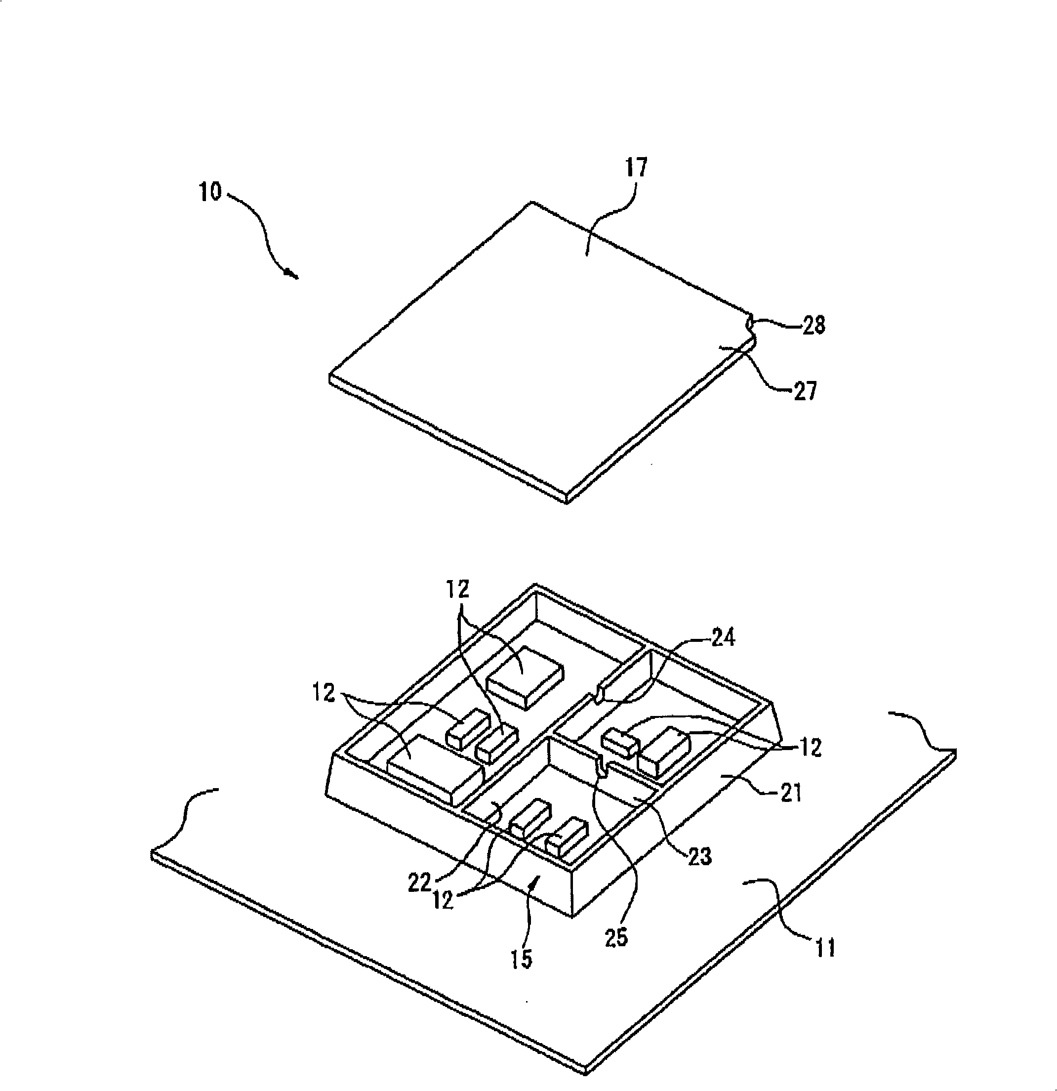
[0094] Figure 5~ Figure 7 The illustrated substrate structure 50 of the third embodiment has a cover portion 51 instead of the cover portion 17 of the first embodiment, and the other configurations are the same as those of the substrate structure 10 of the first embodiment.

[0095] The cover portion 51 is formed with a plurality of injection ports 52 . The plurality of injection ports 52 communicate with the inside of the outer frame 21 (that is, the inside of the frame body 15 ).

[0096] Thus, the inside of the frame body 15 communicates with the outside of the frame body 15 through the plurality of injection ports 52 .

[0097] Next, refer to Figure 8 ~ Figure 11 The steps of manufacturing the substrate structure 50 of the third embodiment will be described.

[0098] Such as Figure 8 As shown, a plurality of electronic components 12 are mounted on a substrate 11 , and a frame body 15 and a cover portion 51 are provided in a resin portion 13 . In this state, from ab...

no. 4 Embodiment approach

[0109] Figure 12 The substrate structure 60 of the fourth embodiment shown in (A) to (C) is a structure in which the manufacturing method of the substrate structure 50 of the third embodiment is changed. Melted resin 53 is injected into the inside of 15, and its configuration is the same as that of the substrate structure 50 of the third embodiment.

[0110] refer to Figure 12 (A) to (C) describe the steps of manufacturing the substrate structure 60 of the fourth embodiment.

[0111] Such as Figure 12 As shown in (A), a plurality of electronic components 12 are mounted on a substrate 11 and a housing 15 of a resin portion 13 is provided. In this state, it is supplied from above the frame body 15 Image 6 The melted resin 53 for the resin 18 shown is injected into the inside of the frame body 15 .

[0112] The injection of the molten resin 53 is stopped until the molten resin 53 is completely filled into the frame body 15 . That is, the injection amount to the inside o...


PUM


Abstract

A board structure and an electronic device are provided in which a resin part that covers a plurality of electronic parts altogether has shielding characteristics and the mounting strength of the electronic parts mounted on the board can be secured. A board structure (10) comprises a board (11), a plurality of electronic parts (12) mounted along the board (11), and a resin part (13) covering each of the electronic parts (12) with resin (18) and adhering to the board (11). This board structure (10) further comprises a frame (15) surrounding the electronic parts (12) and adhering to the board (11) and a cover (17) closing an opening (16) of the frame (15). The resin (18) is placed inside the frame (15).

Description

technical field [0001] The present invention relates to a substrate structure and electronic equipment, wherein a plurality of electronic components are mounted along the substrate, each electronic component is covered with a resin portion, and the resin portion is bonded to the substrate. Background technique [0002] Conventionally, in order to waterproof the electronic components mounted on the substrate, there is known a substrate structure in which the electronic components are covered with a resin portion. [0003] As the resin used in this substrate structure, for example, thermoplastic resins, gel-like silicone resins, and the like are often used. These resins are known to have relatively low elastic moduli after curing. [0004] Therefore, such a substrate structure has disadvantages in that the cured resin cannot withstand impacts such as a drop test, and it is difficult to ensure the mounting strength of the electronic component on the substrate. [0005] On the...

Claims


Application Information

Patent Timeline
Patent Type & Authority Applications(China)
IPC IPC(8): H05K3/28
CPCH05K2201/10371H05K3/284H05K1/0218H05K7/20463H01L2224/16225H01L2924/19105H05K2201/2018H05K2201/09972H05K9/0083H01L2924/00014H01L2924/00011H01L23/552H01L21/565H01L21/56H01L23/053H01L23/3121H01L2224/0401H05K3/28
Inventor 小野正浩宇田吉博山口盛司新地和博留河悟
Owner PANASONIC CORP
Why Eureka
Try Eureka