Semiconductor device

A semiconductor and device technology, applied in the field of semiconductor devices, can solve the problems of reduced solder welding area, difficulty in ensuring installation strength, and reduction in installation strength, and achieve the effect of realizing the installation area and ensuring the installation strength

Inactive Publication Date: 2016-04-06
RENESAS ELECTRONICS CORP
View PDF7 Cites 4 Cited by
  • Summary
  • Abstract
  • Description
  • Claims
  • Application Information

AI Technical Summary

Problems solved by technology

[0011] In the above-mentioned semiconductor devices, in order to cope with the narrower pitch and the reduction of the mounting area, shortening the lead length is considered. However, if the lead length is shortened, the solder bonding area of ​​the lead wire to the mounting substrate will decrease, so there is a concern that the mounting strength will decrease.
[0012] In other words, if the length of the lead wire is shortened, it will be difficult to ensure the mounting strength

Method used


Image

  • Semiconductor device
  • Semiconductor device
  • Semiconductor device

Examples


Embodiment approach

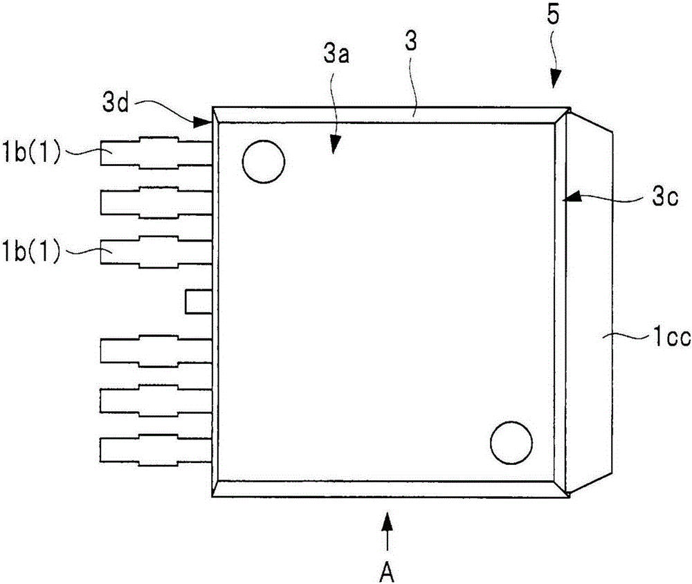
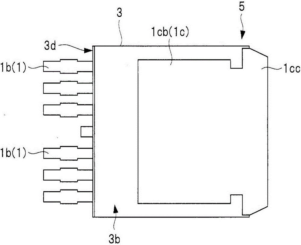
[0077] figure 1 It is a plan view showing an example of the structure of the semiconductor device of the embodiment, figure 2 From figure 1 The view from the direction A shown, image 3 yes means figure 1 A rear view showing an example of the structure of the back side of the semiconductor device, Figure 4 is expressed in perspective figure 1 A perspective top view of the configuration of the interior of the semiconductor device is shown. in addition, Figure 5 is along Figure 4 A cross-sectional view of an example of the structure cut off by the A-A line, Image 6 is along Figure 4 A cross-sectional view and a partially enlarged cross-sectional view of an example of a structure cut along the B-B line of .

[0078]

[0079] Figure 1 to Figure 6 The shown semiconductor device of this embodiment is a semiconductor package including a sealing body 3 that seals a semiconductor chip (also called a pellet) 2 and is formed of an insulating resin, and further has a 3...

Deformed example 1

[0229] In the above embodiments, the structure in which the plurality of outer lead portions 1b protrude from the side surface of the sealing body 3 of the semiconductor device has been described, but the semiconductor device may be, for example, Figure 31 and Figure 32 QFP20 shown.

[0230] here, Figure 31 is a plan view showing the structure of a semiconductor device according to a modified example of the embodiment, Figure 32 is along Figure 31 Cross-sectional view of the construct truncated by line A-A.

[0231] That is, the semiconductor device of this embodiment may also be Figure 31 and Figure 32 shown in the QFP20, at this time, with Figure 7 The shape of the outer lead portion 1b shown is similar, and the distance (length) L2 between the third intersection portion 1h and the fourth intersection portion 1i of the outer lead portion 1b is formed to be larger than that of the first intersection portion 1f of the outer lead portion 1b. The distance (length)...

Deformed example 2

[0234] The solder for the plating film formed in the external plating process of the above-mentioned embodiment, or the solder 9 which is an example of the die-bonding material 6, or the solder 9 used for solder bonding at the time of semiconductor device mounting does not substantially contain lead (Pb). The case of lead-free solder was described, but the above-mentioned solder may be lead-containing solder. However, in consideration of environmental pollution, it is preferable to use a solder formed of the above-mentioned lead-free solder.

[0235] Here, the lead-free solder refers to a solder with a lead (Pb) content of 0.1 wt % or less, which is determined in accordance with the RoHS (Restriction of Hazardous Substances: Restriction of the Use of Certain Hazardous Substances in Electrical and Electronic Equipment) directive.


PUM


Abstract

A semiconductor device is disclosed in the invention to reduce a mounting area while securing a mounting strength of a semiconductor device, a power transistor includes a chip mounting portion, a semiconductor chip, a plurality of leads, and a sealing body. An outer lead portion in each of the plurality of leads includes a first portion protruding from a second side surface of the sealing body in a first direction, a second portion extending in a second direction intersecting with the first direction, and a third portion extending in a third direction intersecting with the second direction. Furthermore, a length of the third portion in the third direction of the outer lead portion is shorter than a length of the first portion in the first direction.

Description

technical field [0001] The present invention relates to a semiconductor device, for example, to an effective technique applicable to a semiconductor device including leads protruding from the side surface of a sealing body that seals a semiconductor chip. Background technique [0002] In recent years, resin-molded semiconductor devices (packages) have been required to reduce the mounting area of ​​packages. [0003] Here, in a semiconductor device having a sealing resin layer sealing a semiconductor chip, for example, Japanese Patent Application Laid-Open No. 5-36863 (Patent Document 1) discloses a structure in which outer leads protruding from the side surfaces of the sealing resin layer are bent, And solder mounting structure to the substrate. [0004] Also, among semiconductor elements having a sealing body, for example, Japanese Patent Laid-Open No. 5-21683 (Patent Document 2) discloses a structure in which leads protruding from the sealing body are bent, and a solderin...

Claims


Application Information

Patent Timeline
Patent Type & Authority Applications(China)
IPC IPC(8): H01L23/49H01L23/04H01L23/13
CPCH01L23/49555H01L23/49562H01L2224/32013H01L2924/181H01L24/97H01L2223/54486H01L2224/0603H01L2224/32245H01L2224/48247H01L2224/48472H01L2224/4903H01L2224/49111H01L2224/49112H01L2224/73265H01L23/544H01L2223/54433H01L2924/13091H01L21/561H01L2224/97H01L2924/00012H01L2924/00H01L23/04H01L23/49541
Inventor 田平幸德小池信也清原俊范
Owner RENESAS ELECTRONICS CORP
Why Eureka
Try Eureka