Diode absorption circuit for bridge rectifier circuit
A technology of bridge rectifier circuit and snubber circuit, which is applied in the electronic field and can solve the problem of large loss of snubber resistor R1
- Summary
- Abstract
- Description
- Claims
- Application Information
AI Technical Summary
Problems solved by technology
Method used
Image
Examples
Embodiment 1
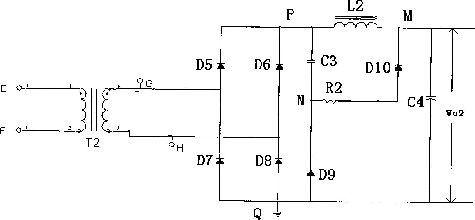
[0021] Diode snubber circuits used in bridge rectifier circuits such as image 3 As shown, the diode snubber circuit is composed of C3, D9, R2, and D10. C3 is generally a non-inductive absorbing capacitor between 1nF and 10nF, and R2 is generally a absorbing resistor ranging from 10 ohms to 100 ohms. D9 and D10 cooperate with C3 and R2 to complete the absorbing function. L2 is a filter inductor, which together with the filter capacitor C4 completes the smooth filtering of the pulsating voltage after bridge rectification on the secondary side of the transformer to ensure that the output voltage Vo2 is a smooth DC.
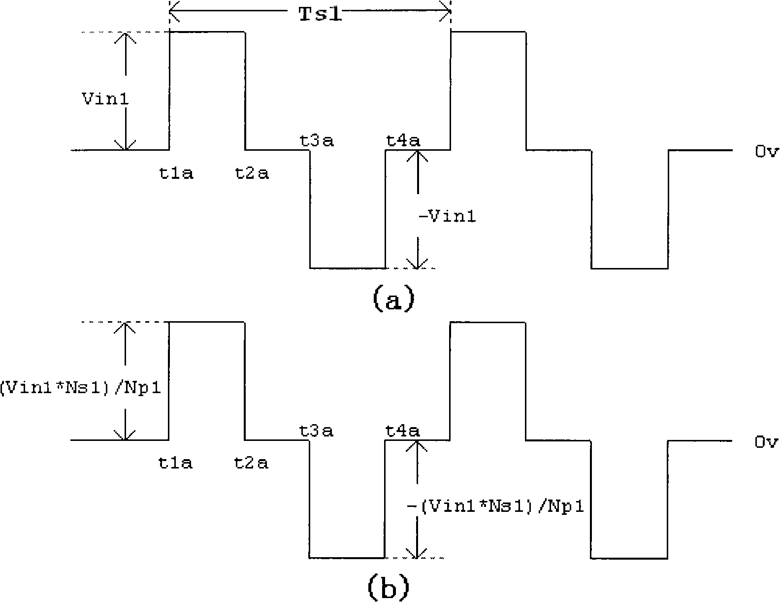
[0022] In this example, the primary and secondary side voltage waveforms of transformer T2 are as follows Figure 4 shown.
[0023] The advantage of the diode snubber circuit in this example is that the loss on the resistor R2 is smaller than that of the traditional circuit, and the snubber effect is almost the same. The specific analysis is as follows:
[0024]...
PUM
 Abstract
Description
Claims
Application Information


