Semiconductor device and method for fabricating the same
A semiconductor and device technology, applied in the field of semiconductor devices, can solve problems such as deterioration of refresh characteristics, reduction of data storage performance of DRAM cells, increase of leakage current in drain regions, etc.
- Summary
- Abstract
- Description
- Claims
- Application Information
AI Technical Summary
Problems solved by technology
Method used
Image

Examples
Embodiment Construction
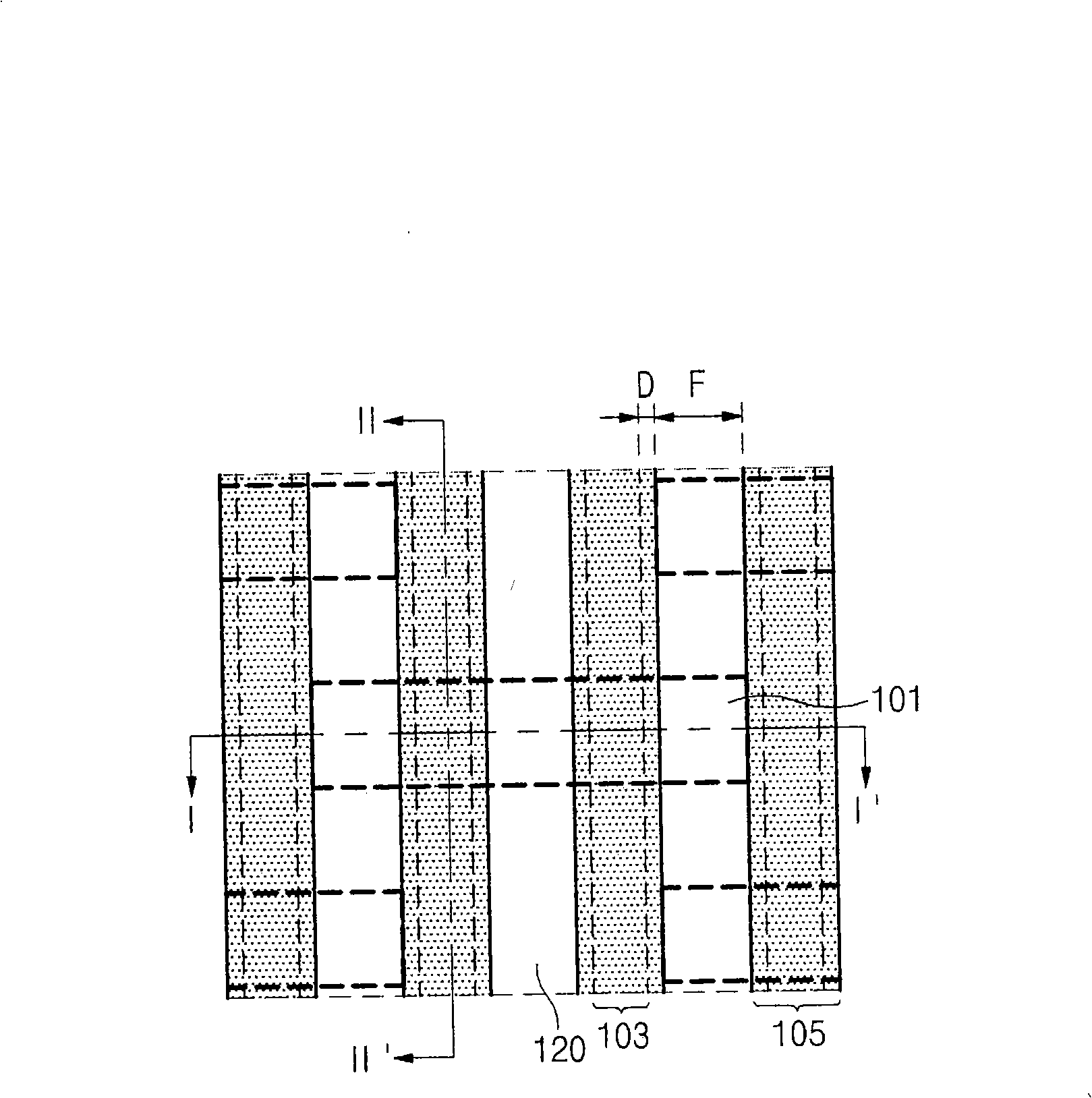
[0013] figure 1 is a layout showing a semiconductor device according to an embodiment of the present invention. The semiconductor device includes an active region 101 defined by a device isolation region 120 , a recessed gate region 103 , and a gate region 105 . The longitudinal direction of the gate region 105 is defined as "vertical direction", and the longitudinal direction of the active region 101 is defined as "horizontal direction". The recessed gate region 103 and the gate region 105 overlap. The figure shows that the horizontal line width of one side of the recessed gate region 103 is smaller than F by D (wherein, 0≦D<F / 2, and F is the distance between two adjacent gate regions 105 ). In other words, the horizontal line width of the recessed gate region 103 is F-2D.
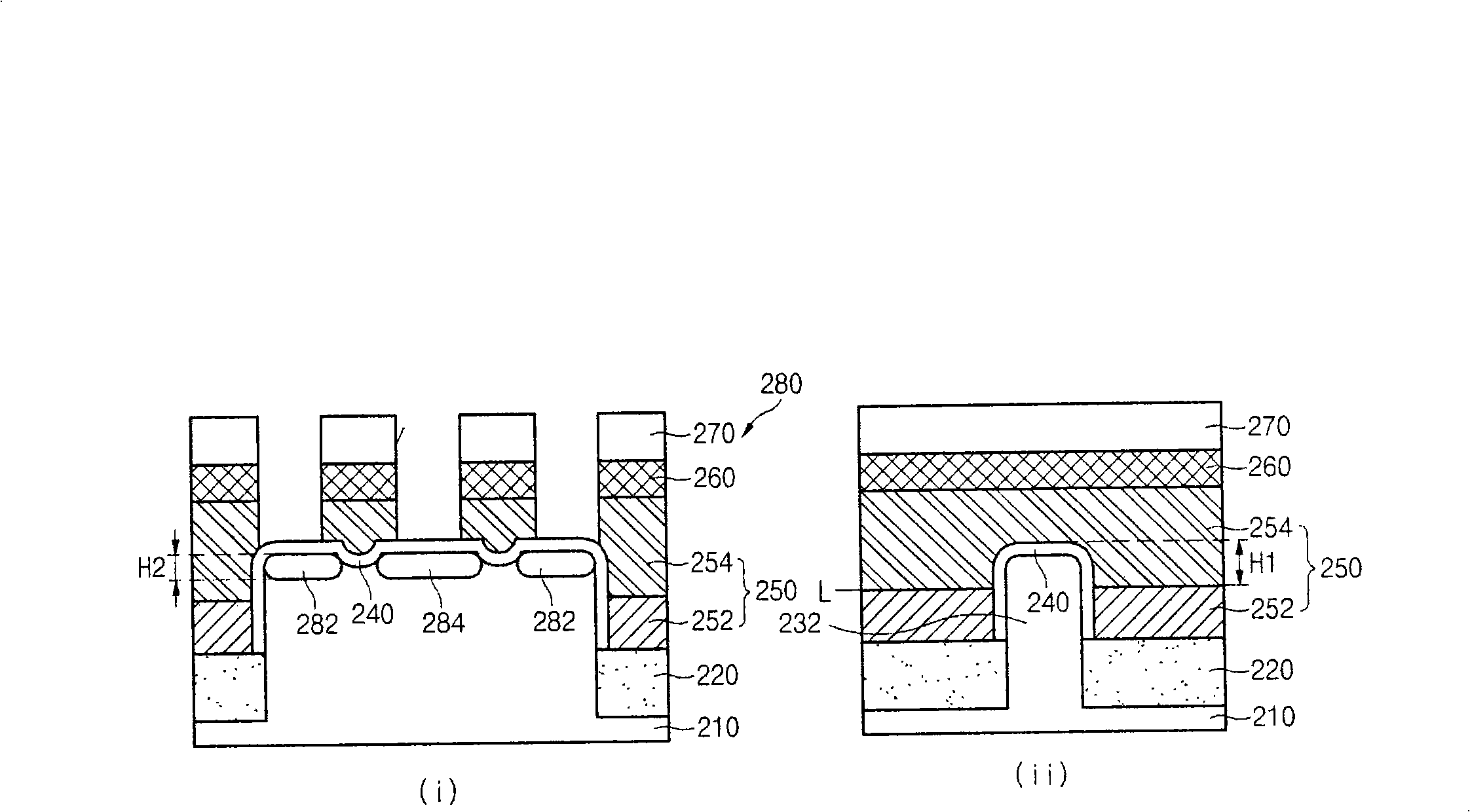
[0014] figure 2 is a cross-sectional view showing a semiconductor device according to an embodiment of the present invention. figure 2 (i) is along figure 1 The cross-sectional view taken by I-I′,...
PUM
 Abstract
Description
Claims
Application Information
 - R&D Engineer
- R&D Manager
- IP Professional
- Industry Leading Data Capabilities
- Powerful AI technology
- Patent DNA Extraction
Browse by: Latest US Patents, China's latest patents, Technical Efficacy Thesaurus, Application Domain, Technology Topic.
© 2024 PatSnap. All rights reserved.Legal|Privacy policy|Modern Slavery Act Transparency Statement|Sitemap