Clock frequency dividing method based on trigger ring and clock frequency dividing circuit thereof

A clock frequency dividing and frequency dividing circuit technology, applied in the synchronous pulse counter, continuous cycle pulse counter, etc., can solve the problems of inaccurate frequency dividing number, large scale of multi-stage frequency dividing circuit, and inoperable frequency dividing circuit, etc. Achieve the effect of small delay and reduced scale

Inactive Publication Date: 2008-10-22
VIMICRO CORP
View PDF0 Cites 14 Cited by
  • Summary
  • Abstract
  • Description
  • Claims
  • Application Information

AI Technical Summary

Problems solved by technology

[0023] The delay of each level of combinational logic can be estimated, assuming it is 0.3ns, and the timing requirement of the flip-flop is 0.7ns. From this calculation, the delay of the whole circuit is 0.3×5+0.7=2.2ns, In other words, the highest frequency that such a circuit can work is 454MHz. If the clock frequency of the PLL is higher than 454MHz, the usual...

Method used


Image

  • Clock frequency dividing method based on trigger ring and clock frequency dividing circuit thereof
  • Clock frequency dividing method based on trigger ring and clock frequency dividing circuit thereof
  • Clock frequency dividing method based on trigger ring and clock frequency dividing circuit thereof

Examples


Embodiment Construction

[0041] The present invention will be described in detail below with reference to the accompanying drawings.

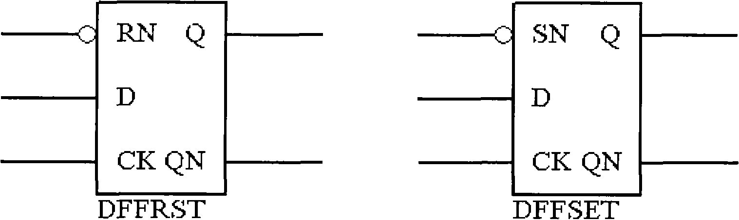
[0042] A flip-flop is a memory device in a circuit. The structure of a common flip-flop with a reset terminal / set terminal is as follows: figure 2 shown. D is the data input terminal, CK is the clock terminal, RN / SN is the reset terminal / set terminal, and Q / QN is the data output terminal. The basic function of the flip-flop is that when RN / SN is 0, the output of Q remains 0 / 1. When RN is not 0, the value of D is latched into Q at the rising edge of each CK. , while QN remains the inverse of Q at all times. Different initial values ​​can be achieved by selecting flip-flops with set or reset terminals.

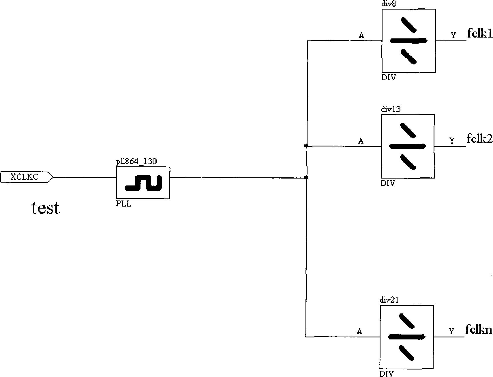
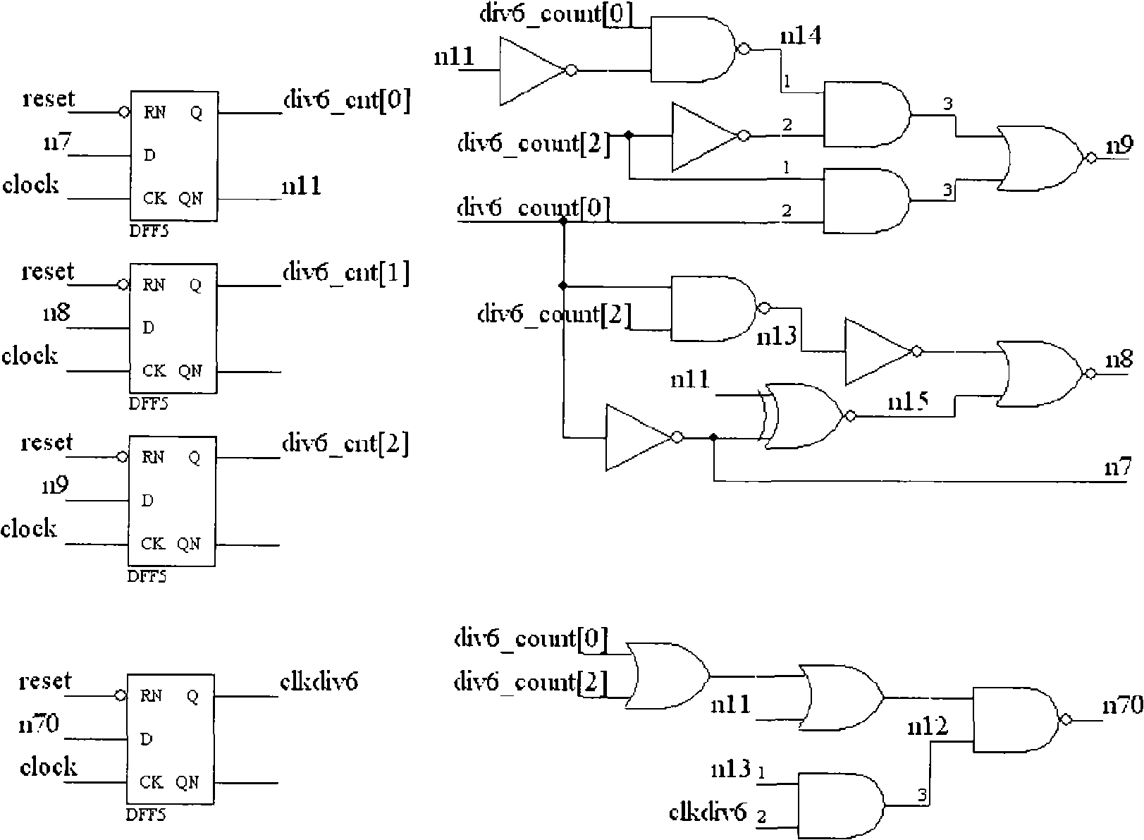
[0043] The clock frequency dividing method based on the flip-flop loop provided by the present invention is to connect the D terminals and Q terminals of several flip-flops in sequence, and the Q terminal of the last flip-flop is connected to the D terminal of the fi...


PUM


Abstract

The present invention relates to a clock frequency division technology for an integrated circuit, in particular to a clock frequency division method based on a trigger ring and a clock frequency division circuit thereof. The method is to orderly connect data input ends and data output ends of a plurality of triggers to form a trigger ring circuit. The number of the triggers with set ends and reset ends in the trigger ring is selected according to the requirement of the frequency division circuit for a duty ratio. The positions of the triggers with set ends and reset ends are determined according to the requirement of a clock waveform. The trigger ring circuit accesses a system frequency division circuit, and a spare data output end of the last trigger is used as an output end of the trigger ring circuit so as to realize clock frequency division. The number of the frequency division of the method and the circuit structure thereof do not influence the highest frequency of the working circuit. The normal work of the frequency division circuit can be at a comparatively high clock frequency, and the clock frequency division can be realized in the manner of cascade connection of the frequency division circuit so that the scale of the circuit realization can be properly reduced.

Description

technical field [0001] The invention relates to a clock frequency dividing technology of an integrated circuit, in particular to a clock frequency dividing method based on a flip-flop ring and a clock frequency dividing circuit thereof. Background technique [0002] Clock frequency divider circuits are very common in the design of integrated circuits. Because the pad of the chip often cannot input a very high frequency clock, or there is no high frequency clock source outside the chip, a low frequency clock, such as 12M, is often input from the pad. The clock is connected to the input of the internal phase-locked loop. The phase-locked loop is a frequency multiplier circuit that can generate a high-frequency clock, such as a 480M clock, based on a lower-frequency input clock. Based on the consideration of function or power consumption, area and timing, one or more functional clocks (fclk1, fclk2, ....) are often needed inside the chip. The clock frequency dividing circuit is...

Claims


Application Information

Patent Timeline
IPC IPC(8): H03K23/54
Inventor 杨柱
Owner VIMICRO CORP
Why Eureka
Try Eureka