Image element structure and production method of display panel
A technology of pixel structure and display panel, which is applied in semiconductor/solid-state device manufacturing, optics, instruments, etc., can solve the problems of decreasing aperture ratio and affecting display effect, and can increase aperture ratio, reduce occupied area, and improve capacitance. Effect
- Summary
- Abstract
- Description
- Claims
- Application Information
AI Technical Summary
Problems solved by technology
Method used
Image

Examples
Embodiment Construction
[0036] In order to enable those who are familiar with the technical field of the present invention to further understand the present invention, several preferred embodiments of the present invention are enumerated below, and in conjunction with the attached drawings, the constitutional content and intended achievement of the present invention are described in detail. effect.
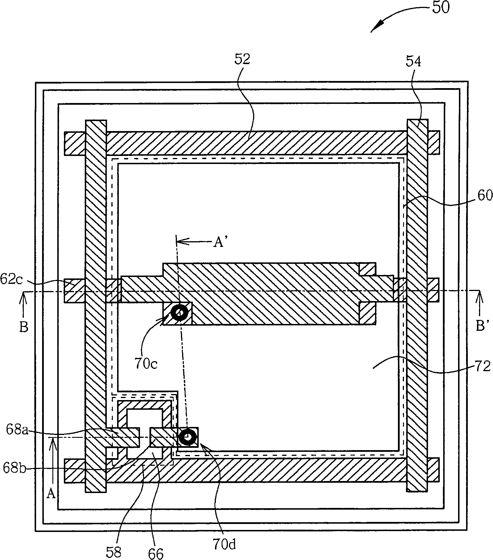
[0037] Please refer to Figure 2a , Figure 2b , Figure 3 and Figure 4. Figure 2a , Figure 2b , FIG. 3 and FIG. 4 are schematic diagrams of a preferred embodiment of the pixel structure of the display panel of the present invention, wherein Figure 2a and Figure 2b They are the top views of the two implementation states of the pixel structure of this embodiment, and Fig. 3 and Fig. 4 are respectively the Figure 2a and Figure 2b The cross-sectional schematic diagram of the section lines AA' and BB'; in addition, each embodiment of the present invention uses the pixel structure of the liquid crystal...
PUM
 Abstract
Description
Claims
Application Information
 - R&D
- Intellectual Property
- Life Sciences
- Materials
- Tech Scout
- Unparalleled Data Quality
- Higher Quality Content
- 60% Fewer Hallucinations
Browse by: Latest US Patents, China's latest patents, Technical Efficacy Thesaurus, Application Domain, Technology Topic, Popular Technical Reports.
© 2025 PatSnap. All rights reserved.Legal|Privacy policy|Modern Slavery Act Transparency Statement|Sitemap|About US| Contact US: help@patsnap.com