Liquid crystal panel and liquid crystal display
A liquid crystal panel and liquid crystal cell technology, applied in optics, instruments, nonlinear optics, etc., can solve problems such as screen contrast, reduce chromatic aberration, suppress uneven display, etc., achieve excellent screen contrast, improve screen contrast, and small chromatic aberration. Effect
- Summary
- Abstract
- Description
- Claims
- Application Information
AI Technical Summary
Problems solved by technology
Method used
Image
Examples
Embodiment 1
[0185] (Formation of the first optical compensation layer)
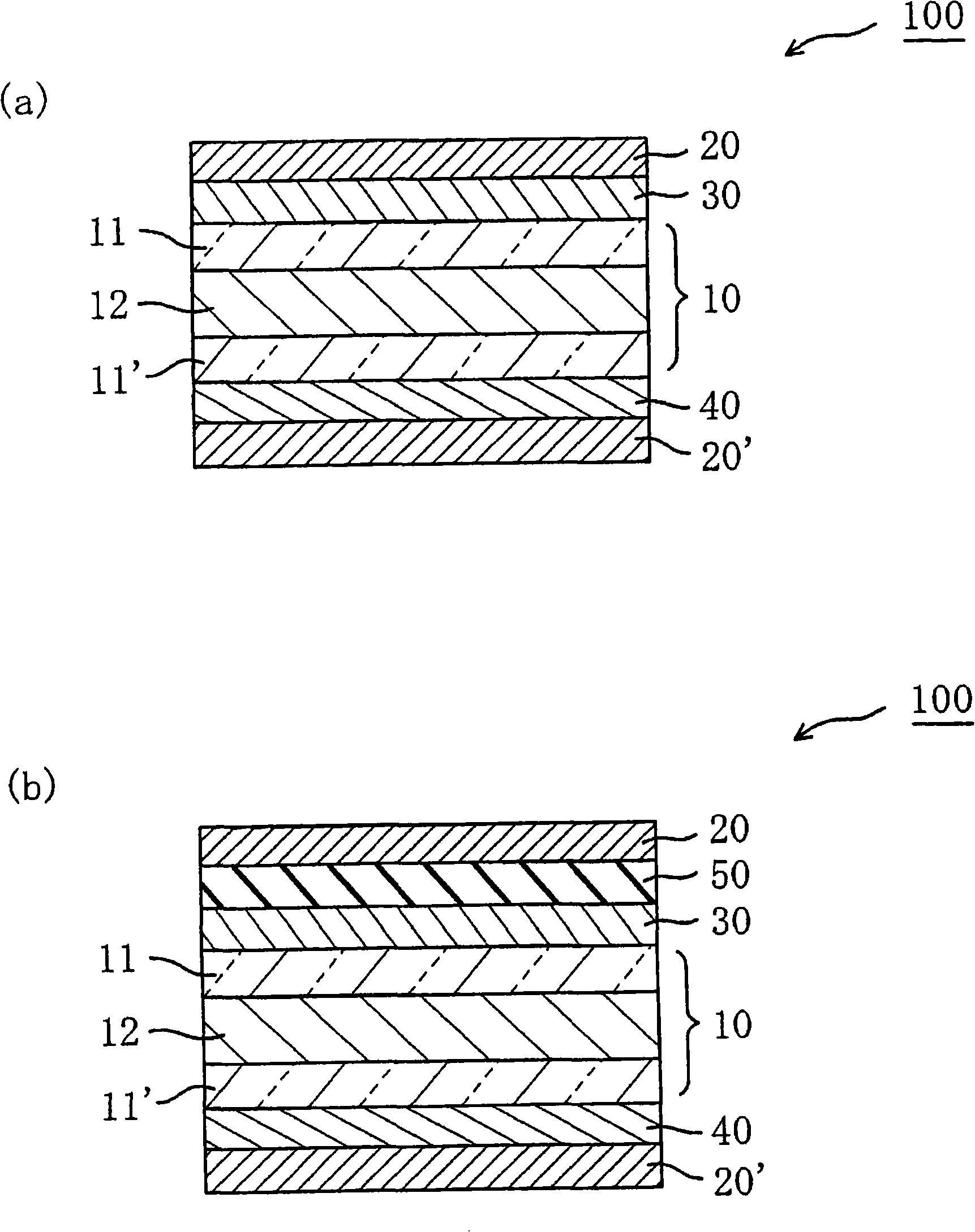
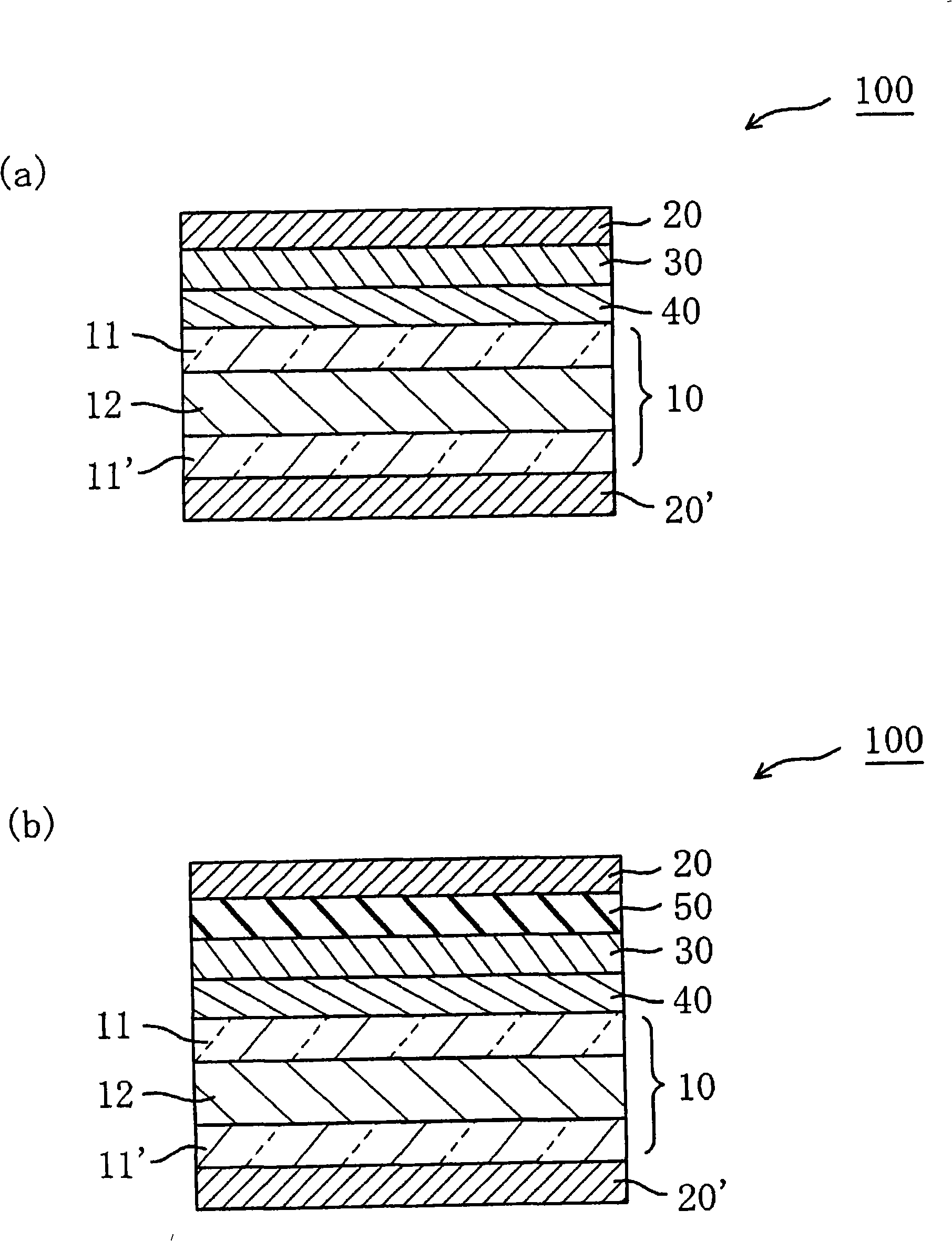
[0186] A film of cellulose ester having a thickness of 70 μm [manufactured by Kaneka Corporation, trade name: KA, DSac (degree of acetyl substitution)=0.04, DSpr (degree of substitution of propionyl group)=2.76] was stretched free-end by 1.5 at 145° C. times to obtain a first optical compensation layer with a thickness of 68 μm. The photoelastic modulus of the obtained first optical compensation layer is 25×10 -12 (m 2 / N). The in-plane retardation of the obtained first optical compensation layer was Δnd(380)=65nm, Δnd(550)=90nm, Δnd(780)=105nm, and the retardation in the thickness direction was Rth(380)=69nm, Rth( 550) = 95 nm, Rth (780) = 111 nm. The refractive index profile at 550nm is
[0187] (Manufacture of polarizing plate with first optical compensation layer)
[0188] The above-obtained first optical compensation layer was bonded to a TAC protective film (manufactured by Fujifilm Corporation, trade n...
Embodiment 2
[0196] (Formation of the first optical compensation layer)
[0197] A cellulose ester film [manufactured by Kaneka Corporation, trade name: KA] having a thickness of 70 μm was stretched 1.45 times at the free end at 145° C. to obtain a first optical compensation layer. The photoelastic modulus of the obtained first optical compensation layer is 25×10 -12 (m 2 / N). The in-plane retardation of the obtained first optical compensation layer was Δnd(380)=58nm, Δnd(550)=80nm, Δnd(780)=93nm, and the retardation in the thickness direction was Rth(380)=65nm, Rth( 550)=90nm, Rth(780)=105nm. The refractive index profile at 550nm is
[0198] (Formation of the second optical compensation layer)
[0199] 2,2-bis(3,4-dicarboxyphenyl)hexafluoropropane dianhydride (6FDA) and 2,2'-bis(trifluoromethyl)-4,4'-diaminobiphenyl (TFMB) The synthesized polyimide was dissolved in methyl isobutyl ketone (MIBK) to prepare a 15% by mass polyimide solution. This solution was coated on a triacetylce...
Embodiment 3
[0202] (Formation of the first optical compensation layer)
[0203] A cellulose ester film [manufactured by Kaneka Corporation, trade name: KA] having a thickness of 70 μm was stretched 1.55 times at the free end at 145° C. to obtain a first optical compensation layer. The photoelastic modulus of the obtained first optical compensation layer is 25×10 -12 (m 2 / N). The in-plane retardation of the obtained first optical compensation layer was Δnd(380)=73nm, Δnd(550)=100nm, Δnd(780)=117nm, and the retardation in the thickness direction was Rth(380)=76nm, Rth( 550)=105nm, Rth(780)=123nm. The refractive index profile at 550nm is
[0204] (Formation of the second optical compensation layer)
[0205] 2,2-bis(3,4-dicarboxyphenyl)hexafluoropropane dianhydride (6FDA) and 2,2'-bis(trifluoromethyl)-4,4'-diaminobiphenyl (TFMB) The synthesized polyimide was dissolved in methyl isobutyl ketone (MIBK) to prepare a 15% by mass polyimide solution. This solution was coated on a triacety...
PUM
| Property | Measurement | Unit |
|---|---|---|
| number average molecular weight | aaaaa | aaaaa |
Abstract
Description
Claims
Application Information
 - R&D
- Intellectual Property
- Life Sciences
- Materials
- Tech Scout
- Unparalleled Data Quality
- Higher Quality Content
- 60% Fewer Hallucinations
Browse by: Latest US Patents, China's latest patents, Technical Efficacy Thesaurus, Application Domain, Technology Topic, Popular Technical Reports.
© 2025 PatSnap. All rights reserved.Legal|Privacy policy|Modern Slavery Act Transparency Statement|Sitemap|About US| Contact US: help@patsnap.com


