Electrically programmable fuse

A technology of fuses and heavily doped regions, used in circuits, electrical components, electrical solid devices, etc.

Active Publication Date: 2008-11-05
IBM CORP
View PDF0 Cites 16 Cited by
  • Summary
  • Abstract
  • Description
  • Claims
  • Application Information

AI Technical Summary

Problems solved by technology

Therefore, such a conven...

Method used


Image

  • Electrically programmable fuse
  • Electrically programmable fuse
  • Electrically programmable fuse

Examples


Embodiment Construction

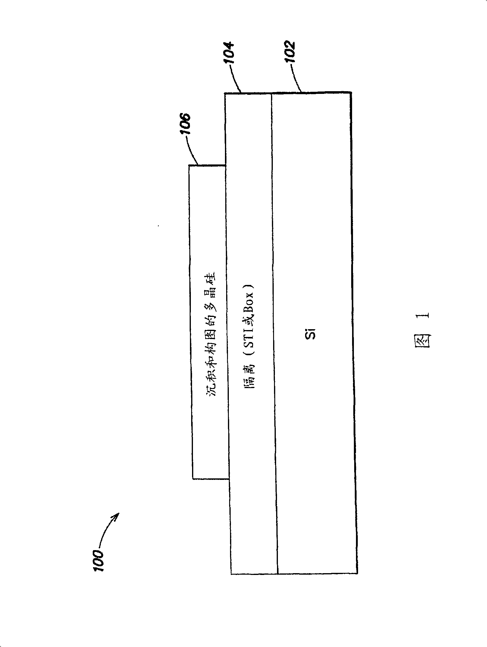
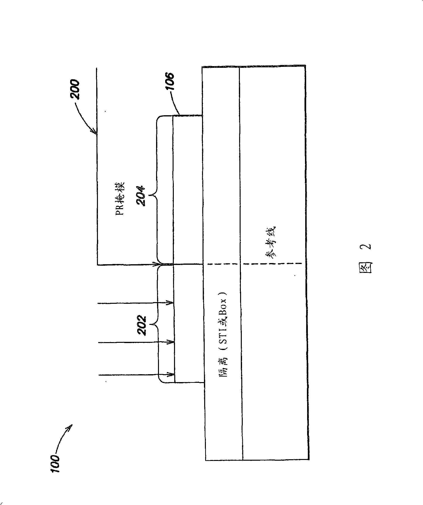
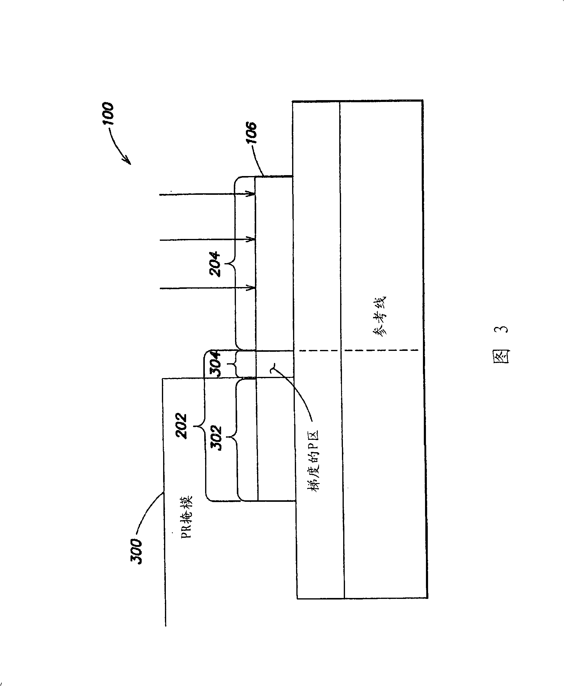
[0028] The present invention provides improved eFuses and methods of making the same. More specifically, the present invention provides a resistance having a length independent of a gap formed in a silicide layer of an eFuse during programming, and a method of manufacturing such an eFuse. The eFuse includes a diode element under the silicide. In some embodiments, the diode element may comprise polysilicon, silicon-on-insulator, or other suitable semiconductor materials. The diode element is reverse biased during read and thus provides a high resistance when the state of the programmed eFuse is sensed. The resulting resistance of the eFuse depends on the formation of the diode and becomes independent of the length of the gap formed in the silicide layer during programming. The characteristics of the reverse diode IV define a resistance several orders of magnitude higher than the magnitude of the length of the mono-doped polysilicon line surrounding the diode portion. Therefo...


PUM


Abstract

An electrically programmable fuse (eFuse) includes (1) a semiconducting layer above an insulating oxide layer of a substrate; (2) a diode formed in the semiconducting layer; and (3) a silicide layer formed on the diode. The diode comprises an N+,p-,P+ or P+,n-,N+ structure.

Description

technical field [0001] The present invention relates generally to semiconductor device fabrication, and more particularly to electrically programmable fuses (eFuses) and methods of fabrication thereof. Background technique [0002] Conventional eFuses may include silicide on a polysilicon layer that acts as a resistor. To program a conventional eFuse, current may be driven in a first direction from the cathode to the anode of the conventional eFuse (eg, through one or more transistors). Driving current in the first direction through the eFuse forms a gap in the silicide layer, thereby exposing a portion of the polysilicon layer. The state of a programmed eFuse can be sensed by attempting to drive current in a second direction from anode to cathode. The resistance of the path through which current is driven depends on the length of the gap formed in the silicide layer during programming. Due to variations in the operating parameters of the transistors and / or the control of...

Claims


Application Information

Patent Timeline
IPC IPC(8): H01L23/525
CPCH01L2924/0002H01L23/5252H01L2924/00H01L23/62H01L23/525
Inventor 许履尘杰克·曼德尔曼威廉·汤蒂
Owner IBM CORP
Why Eureka
Try Eureka