Digital logic chip and method capable of testing design

A technology of digital logic and test design, applied in the direction of measuring electricity, measuring devices, measuring electrical variables, etc., can solve the problems of not being able to observe N signals, not being able to directly observe, etc.

Inactive Publication Date: 2008-11-12
VIMICRO CORP
View PDF0 Cites 11 Cited by
  • Summary
  • Abstract
  • Description
  • Claims
  • Application Information

AI Technical Summary

Problems solved by technology

[0010] It can be seen that N pins are used in the above method, and when the number of chip pins is relatively small (for example, N=3, but only one pin can be used), all N signals cannot be observed
When using N pins, the output of the flip-flop can be directly observed through the pins, so that it can be observed, but if the pins are required to be used less, it cannot be directly observed

Method used


Image

  • Digital logic chip and method capable of testing design
  • Digital logic chip and method capable of testing design
  • Digital logic chip and method capable of testing design

Examples


Embodiment Construction

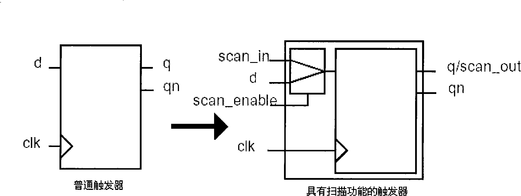
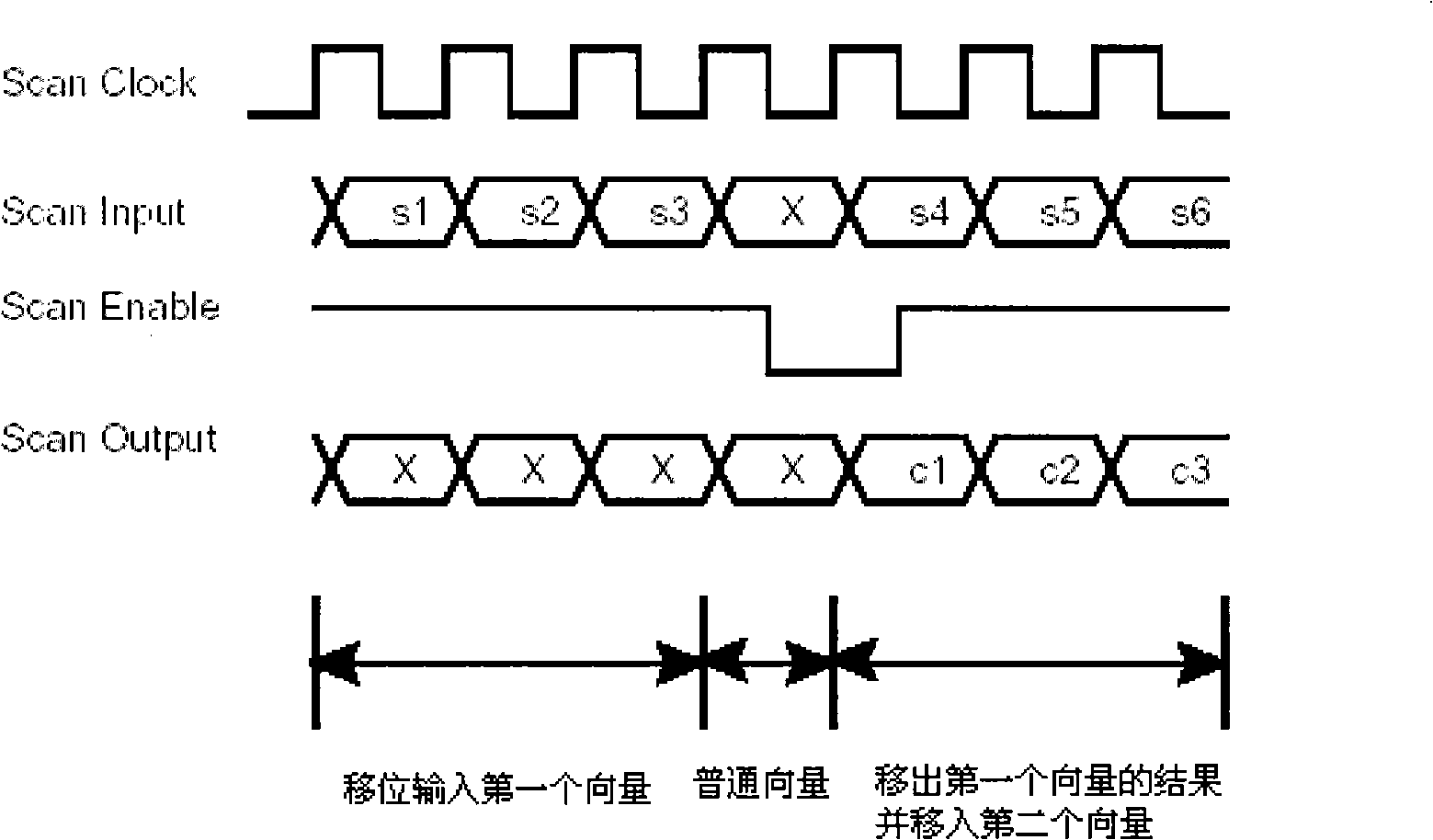
[0033] Hereinafter, the digital logic chip and its testable design method of the present invention will be described in detail with reference to the accompanying drawings.

[0034] Such as Figure 5 Shown, be the method flow chart of digital logic chip testable design of the present invention, this method comprises the following steps:

[0035] Corresponding logic devices are arranged between each scan flip-flop and the observation pin in the digital logic chip;

[0036] Observing the signals of each scan flip-flop in time division through the observation pin;

[0037] After the signal passes through the above-mentioned logic device, it is judged whether the observation result is consistent with the predetermined observation result; if it is consistent, it is considered that the digital logic chip is normal; if it is inconsistent, it is considered that the digital logic chip is abnormal.

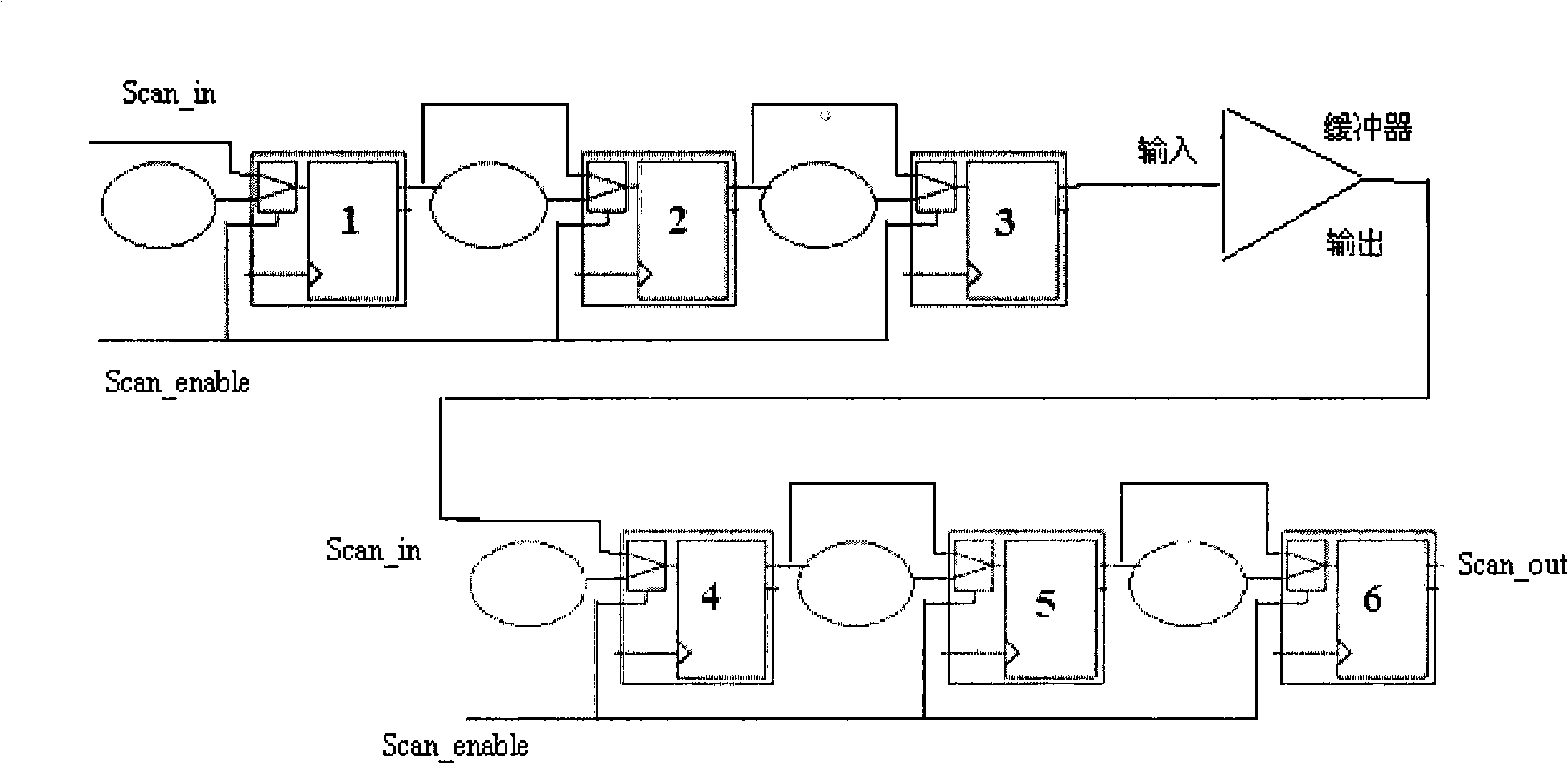
[0038] Such as Figure 6 As shown in , it is a schematic diagram of using a pin pin f...


PUM


Abstract

The invention provides a digital logic chip and a method of design for testing, wherein, the method includes setting corresponding logic devices between each scanning trigger in the digital logic chip and each observing pin, by the observing pin, signal of each scanning trigger can be observed in different time; after the signal pass over the logic device, the observing result is compared with the forecasted observing result so as to determine whether the digital logic chip is normal or not. The digital logic chip of the invention and the method of design for testing can realize the observation of circuit scanning test by adopting few pins.

Description

technical field [0001] The invention relates to the technical field of chips, in particular to a digital logic chip and a testable design method thereof. Background technique [0002] In digital logic chips (such as multimedia processing and control chips), design for testability is usually required. Testability refers to the ability of a circuit to find, isolate, and locate faults, as well as the ability to design and execute tests within a certain time and cost. In other words, testability is the ease with which an integrated circuit can be tested. [0003] At present, a common testable design is scanning testable design, which refers to a method of stimulating the logic unit in the circuit through the scanning method, and scanning the result of the unit operation, so as to judge whether the circuit production is qualified. A common scan testable design is a scan-based testable design (Scan Design For Test, Scan DFT), which is implemented on the circuit by scanning test ...

Claims


Application Information

Patent Timeline
Patent Type & Authority Applications(China)
IPC IPC(8): G01R31/3185
Inventor 王振国
Owner VIMICRO CORP
Why Eureka
Try Eureka