
Image sensor and method for forming the same

An image sensor and device technology, applied in semiconductor/solid-state device manufacturing, electrical components, circuits, etc., can solve problems such as affecting the performance of pixel units, reducing the effective area of ​​photodiodes, etc., to achieve the effect of performance assurance

Inactive Publication Date: 2010-08-18
SEMICON MFG INT (SHANGHAI) CORP
View PDF1 Cites 0 Cited by
  • Summary
  • Abstract
  • Description
  • Claims
  • Application Information

AI Technical Summary

Problems solved by technology

However, with the above technology, since the deep trenches and device isolation layers exist in parallel between adjacent photodiode regions, the effective area of ​​the photodiode is reduced, so the response speed and quality of the pixel unit to light will be reduced, which will affect the performance of the pixel unit.

Method used


Image

  • Image sensor and method for forming the same
  • Image sensor and method for forming the same
  • Image sensor and method for forming the same

Examples


Embodiment Construction

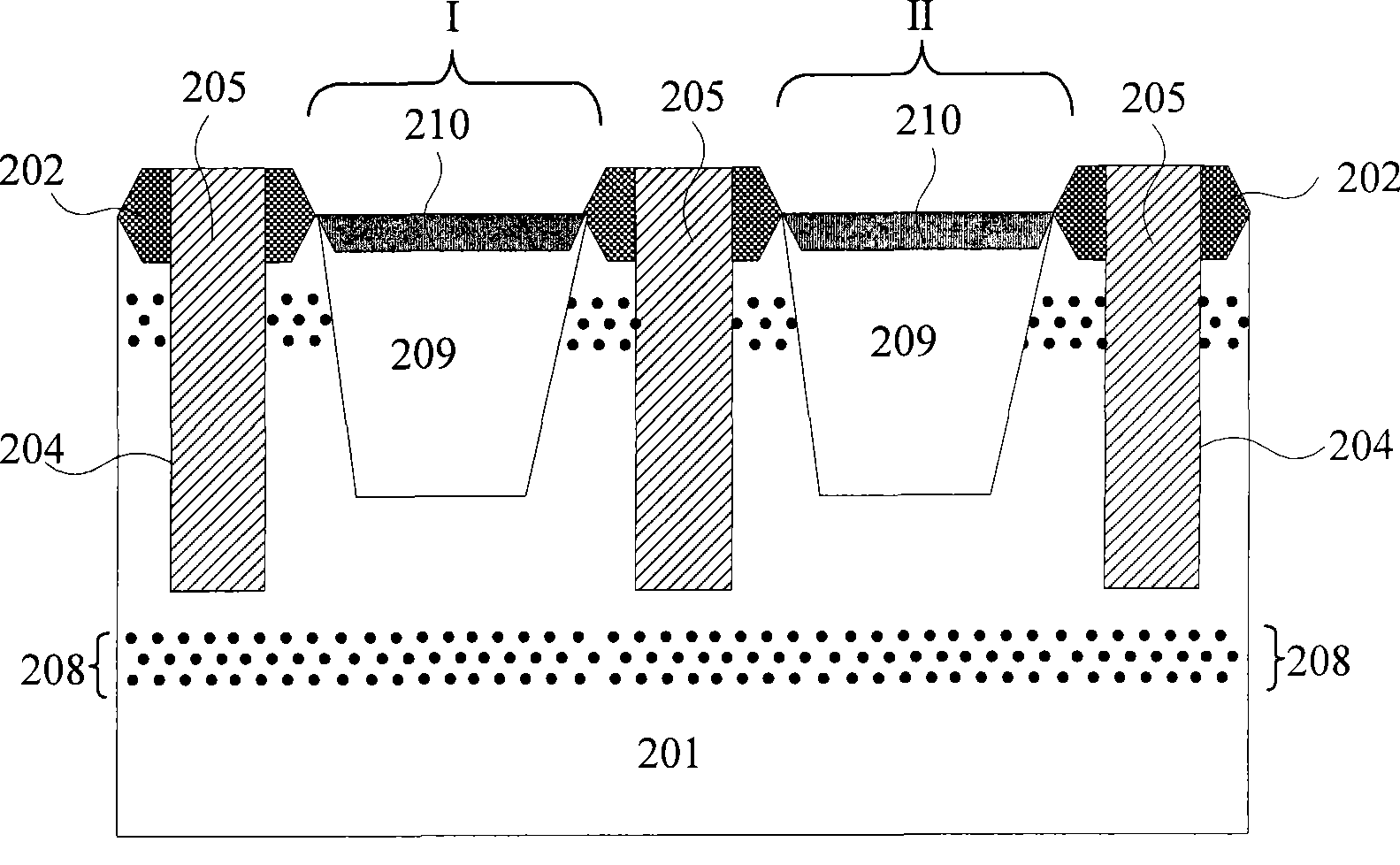
[0031] The present invention provides an image sensor that uses trenches to isolate adjacent photodiode regions. The present invention uses a deep trench to isolate the image sensor, and the deep trench runs through the device isolation layer, and the bottom of the deep trench is located under the first doped well of the photodiode, which can effectively prevent the photodiode region of the adjacent pixel unit region from generating The leakage current, meanwhile, does not reduce the photodiode area, so that the photodiode performance is guaranteed.

[0032] The present invention firstly provides a method for forming an image sensor, including: providing a semiconductor substrate with a first conductivity type, the semiconductor substrate includes a first pixel unit area and a second pixel unit area, and each pixel unit area has a photoelectric Diode region; forming a device isolation layer between the photodiode region of the first pixel unit region and the photodiode region ...


PUM


Abstract

The invention relates to an image sensor which consists of a device isolating layer positioned between photoelectric diode areas of two adjacent pixel unit areas, a first doping trap positioned in the photoelectric diode area under a semiconductor underlayer surface and provided with a first conducting type, a second doping trap provided with a second conducting type and positioned under the first doping trap and a deep groove which is also formed in the semiconductor underlayer and runs through the device isolating layer; the bottom of the deep groove is positioned under the second doping trap. The image sensor has the advantages that the production of drain current in the photoelectric diode area of adjacent pixel units can be effectively prevented by adopting the deep groove to isolatethe photoelectric diode area between the pixel units; meanwhile, as the deep groove runs through the device isolating layer while the bottom of the deep groove is positioned under the first doping trap of the photoelectric diode, the surface of the photoelectric diode area is not reduced, and the performance of the photoelectric diode is guaranteed.

Description

technical field [0001] The invention relates to the field of semiconductor technology, in particular to an image sensor and a forming method thereof. Background technique [0002] At present, the charge coupled device (CCD) is the main practical solid-state image sensor device, which has the advantages of low read noise, large dynamic range, and high response sensitivity. However, CCD also has the disadvantage of being difficult to be compatible with the mainstream Complementary-Metal-Oxide-Semiconductor (CMOS) technology, that is, the CCD-based image sensor is difficult to achieve single-chip integration. The CMOS image sensor (CMOS Image sensor, CIS) adopts the same CMOS technology, and can integrate the pixel cell array and peripheral circuits on the same chip. Compared with CCD, CIS has the advantages of small size, light weight, low power consumption, The advantages of convenient programming, easy control and low average cost. [0003] Generally, a CMOS image sensor i...

Claims


Application Information

Patent Timeline
Patent Type & Authority Patents(China)
IPC IPC(8): H01L21/762H01L21/822H01L27/146
Inventor 霍介光
Owner SEMICON MFG INT (SHANGHAI) CORP
Learn More