Method for preparing LED

A technology for light-emitting diodes and a manufacturing method, which is applied to electrical components, circuits, semiconductor devices, etc., can solve problems such as reduction and insignificant improvement of luminous efficiency, and achieve the effect of ensuring crystal quality.

Inactive Publication Date: 2008-11-12
SHANGHAI INST OF MICROSYSTEM & INFORMATION TECH CHINESE ACAD OF SCI
View PDF0 Cites 10 Cited by
  • Summary
  • Abstract
  • Description
  • Claims
  • Application Information

AI Technical Summary

Problems solved by technology

[0005] However, from the actual situation, the existing single-electrode structure does not significantly increase the luminous efficiency, or even slightly reduces it. The reason is that the compound semiconductor material grown on the silicon substrate or other conductive substrates is used as the light-emitting layer Its crystal quality is far from that of sapphire substrate growth

Method used


Image

  • Method for preparing LED
  • Method for preparing LED
  • Method for preparing LED

Examples


Embodiment Construction

[0022] Below in conjunction with specific embodiment, further illustrate the present invention. It should be understood that these examples are only used to illustrate the present invention and are not intended to limit the scope of the present invention. In addition, it should be understood that after reading the teachings of the present invention, those skilled in the art can make various changes or modifications to the present invention, and these equivalent forms also fall within the scope defined by the appended claims of the present application.

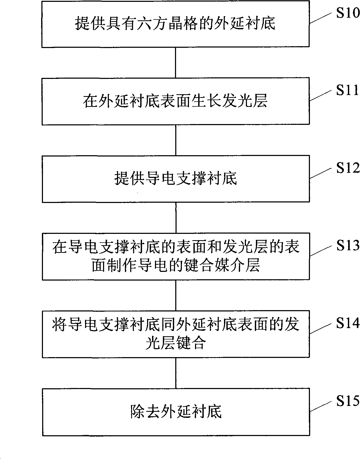
[0023] Such as figure 1 Shown is the implementation process flow chart of the specific embodiment of the manufacturing method of the light emitting diode provided by the present invention. Step S10, providing an epitaxial substrate with a hexagonal lattice; Step S11, growing a light-emitting layer on the surface of the epitaxial substrate; Step S12, providing a conductive support substrate; Step S13, fabricating The conductiv...


PUM


Abstract

The invention relates to a manufacturing method of a light emitting diode (LED), which comprises the following steps: an extending substrate with hexagonal lattices is adopted; an emitting layer is grown on the surface of the extending substrate; conductive supporting substrates are adopted; the conductive supporting substrates are bonded with the emitting layer on the surface of the extending substrate; the extending substrate is then removed. The manufacturing method has the advantages that: the extending substrate with hexagonal lattices is adopted to grow the emitting layer, thus ensuring the crystal quality of the emitting layer; by adopting the method of bonding conductive supporting substrates and then peeling off the extending substrate, the technical problems that the extending substrate is not conductive and vertical structures cannot be made can be solved.

Description

technical field [0001] The invention relates to the field of manufacturing optoelectronic devices, in particular to a method for manufacturing a light emitting diode. Background technique [0002] Light-emitting diode (LED) is a very important light-emitting device in the field of optoelectronics, and is widely used in many fields such as display backlight, general lighting, and medical detection. One of the key factors limiting the further application of LEDs is that the luminous efficiency of LEDs still cannot meet people's needs. Therefore, improving the luminous efficiency of LEDs can promote the wider application of LEDs. [0003] Using sapphire or other substrates with a hexagonal lattice to grow III-V compound semiconductor materials as the light-emitting layer, such as GaAs / InGaAs or GaN / InGaN, and then making LED devices is a common method of making LEDs in the prior art. . Since the sapphire as the substrate is insulated, both electrodes of the LED must be fabric...

Claims


Application Information

Patent Timeline
Patent Type & Authority Applications(China)
IPC IPC(8): H01L33/00
Inventor 陈静孙佳胤王曦
Owner SHANGHAI INST OF MICROSYSTEM & INFORMATION TECH CHINESE ACAD OF SCI
Why Eureka
Try Eureka