

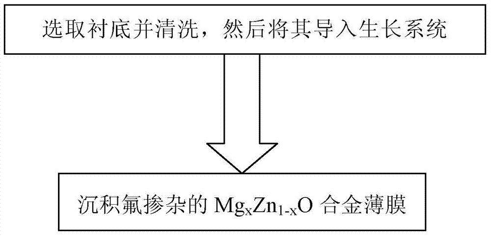
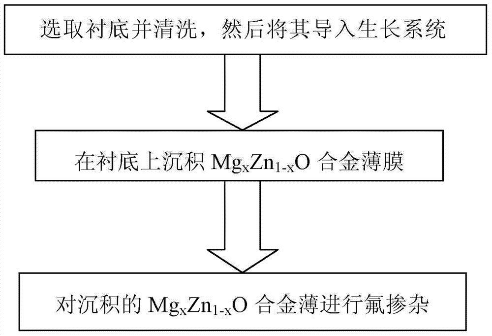
Method for improving the conductivity of MgxZn(1-x)O and application of MgxZn(1-x)O in photoelectronic device
An optoelectronic device, mgxzn1-xo technology, which is applied in semiconductor devices, electrical components, circuits, etc., can solve the problems of hindering the electrical property regulation target of alloy thin films, low substitution doping efficiency, etc., and achieves simple structure, high luminous intensity, The effect of ensuring crystal quality
- Summary
- Abstract
- Description
- Claims
- Application Information
AI Technical Summary
Problems solved by technology
Method used
Image

Examples
Embodiment 1
[0043] Example 1: Preparation of fluorine-doped Mg on a sapphire single crystal substrate by radio frequency plasma-assisted molecular beam epitaxy 0.5 Zn 0.5 O film. Specific steps are as follows:
[0044] The organic matter on the surface of the sapphire single crystal substrate is removed by ultrasonic cleaning such as acetone, alcohol and deionized water, and then introduced into the RF plasma-assisted molecular beam epitaxy system;
[0045] ZnF 2 As a doping source, F-doped Mg was deposited on a sapphire single crystal substrate 0.5 Zn 0.5 O(0001)) layer, the growth conditions are as follows: the substrate temperature is 450°C, the beam current of Mg is 1.9x10 14 atoms / cm 2 s, the beam current of Zn is 2.5x10 14 atoms / cm 2 s, oxygen flow rate 2.6sccm, RF power 340W, ZnF 2 The doping temperature was 420°C, and the deposition time was 2 hours to obtain a film with a thickness of about 270 nm.
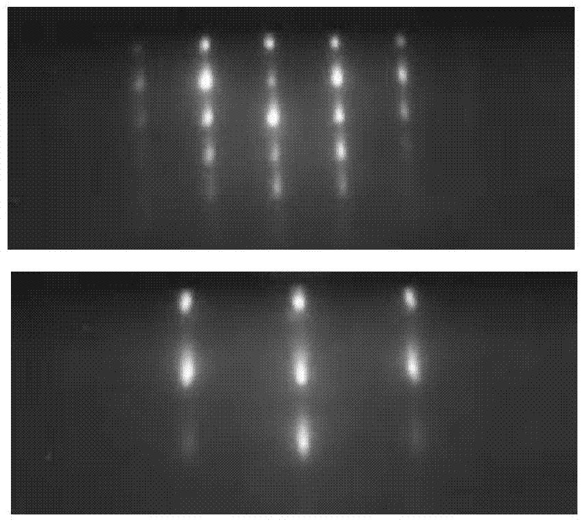
[0046] During the film preparation process, the samples were monitored...
Embodiment 2
[0050] Example 2: Preparation of fluorine-doped Mg on sapphire single crystal substrate by radio frequency plasma assisted molecular beam epitaxy 0.45 Zn 0.55 O film. Specific steps are as follows:
[0051] ZnF 2 As a dopant source, growth of fluorine-doped Mg 0.45 Zn 0.55 O(0001) layer, the growth conditions are: the substrate temperature is 450°C, the beam current of Mg is 1.7x10 14 atoms / cm 2 s, the beam current of Zn is 2.5x10 14 atoms / cm 2 s, oxygen flow rate 2.6sccm, RF power 340W, ZnF 2 The doping temperature was 390°C, and the deposition time was 2 hours to obtain a film with a thickness of about 240 nm.
[0052] RHEED in-situ monitoring results and XRD test show that the prepared film is Mg with high Mg component 0.45 Zn 0.55 O(0001) single crystal sample. Reflection spectrum test results show that the forbidden band width of the film is 4.29eV (corresponding to 289nm), indicating that fluorine-doped Mg 0.45 Zn 0.55 O thin films can be used in ultraviole...
Embodiment 3
[0054] Example 3: Preparation of fluorine-doped Mg on a silicon single crystal substrate by radio frequency plasma assisted molecular beam epitaxy 0.3 Zn 0.7 O film. Specific steps are as follows:
[0055] ZnF 2 As a dopant source, growth of fluorine-doped Mg 0.3 Zn 0.7 O(0001) layer. The growth conditions are: the substrate temperature is 450°C, the beam current of Mg is 1.4x10 14 atoms / cm 2 s, the beam current of Zn is 2.5x10 14 atoms / cm 2 s, oxygen flow rate 2.6sccm, RF power 340W, ZnF 2 The doping temperature was 390°C, and the deposition time was 2 hours to obtain a film with a thickness of about 210 nm.
[0056] RHEED in-situ monitoring results and XRD test show that the prepared film is Mg 0.3 Zn 0.7 O(0001) single crystal sample. Reflection spectrum test results show that the film has a forbidden band width of 3.95eV (314nm), indicating that fluorine-doped Mg 0.3 Zn 0.7 O thin films can be used in ultraviolet detectors.
[0057] The electrical propertie...
PUM
 Abstract
Description
Claims
Application Information