Preparation method of epitaxial wafer of light emitting diode

A technology for light-emitting diodes and epitaxial wafers, applied in electrical components, circuits, semiconductor devices, etc., can solve the problems of low luminous efficiency of light-emitting diodes, and achieve the effects of improving luminous efficiency, ensuring crystal quality, and reducing light absorption.

Inactive Publication Date: 2019-05-24
HC SEMITEK ZHEJIANG CO LTD
View PDF0 Cites 1 Cited by
  • Summary
  • Abstract
  • Description
  • Claims
  • Application Information

AI Technical Summary

Problems solved by technology

However, the current epitaxial wafer is limited by the defects in the epitaxial wafer and the hole concent

Method used


Image

  • Preparation method of epitaxial wafer of light emitting diode
  • Preparation method of epitaxial wafer of light emitting diode
  • Preparation method of epitaxial wafer of light emitting diode

Examples


Embodiment Construction

[0028] In order to make the object, technical solution and advantages of the present invention clearer, the implementation manner of the present invention will be further described in detail below in conjunction with the accompanying drawings.

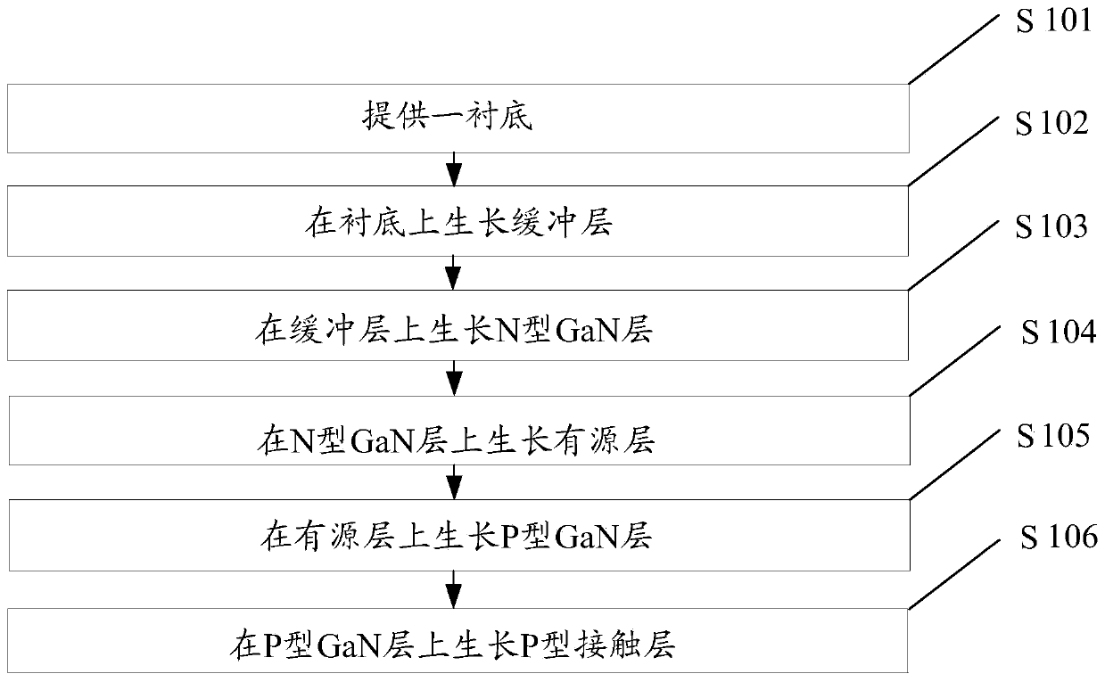
[0029] figure 1 It is a flow chart of a method for preparing an epitaxial wafer of a light-emitting diode provided by an embodiment of the present invention, such as figure 1 Shown, this preparation method comprises:

[0030] S101: Provide a substrate.

[0031] S102: growing a buffer layer on the substrate.

[0032] S103: growing an N-type GaN layer on the buffer layer.

[0033] S104: growing an active layer on the N-type GaN layer.

[0034] S105: growing a P-type GaN layer on the active layer.

[0035] S106: growing a P-type contact layer on the P-type GaN layer.

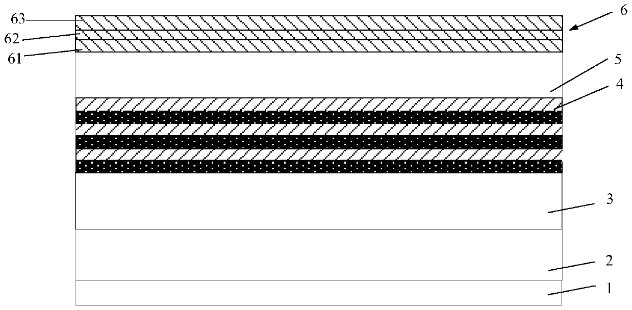
[0036] The doping element in the P-type contact layer is Mg, and the P-type contact layer includes a first P-type contact sublayer, a second P-type contact sublayer, ...


PUM

PropertyMeasurementUnit
Growth thicknessaaaaaaaaaa

Abstract

The invention discloses a preparation method of an epitaxial wafer of a light emitting diode, which belongs to the field of light emitting diode manufacturing. The growth temperature of a second P-type contact sub-layer in a P-type contact layer is 650-750 DEG C. The growth can increase the amount of Mg doped in the second P-type contact sub-layer, increase the number of holes in the P-type contact layer, increase the number of holes injected into an active layer and improve the luminescence efficiency of the light emitting diode. The increase of the amount of Mg doped in the second P-type contact sub-layer enables a good ohmic contact to be formed between the P-type contact layer and a P electrode, increases current expansion and reduces the working voltage of the light emitting diode. The growth temperature of a first P-type contact sub-layer is higher than that of the second P-type contact sub-layer, which can ensure the quality of the second P-type contact sub-layer. The growth temperature of a third P-type contact sub-layer is higher than that of the second P-type contact sub-layer, which can reduce the amount of carbon impurities doped in the third P-type contact sub-layer, reduce the overall light absorption of the P-type contact layer and improve the luminescence efficiency of the light emitting diode.

Description

technical field [0001] The invention relates to the field of light-emitting diode manufacturing, in particular to a method for preparing an epitaxial wafer of a light-emitting diode. Background technique [0002] LED (Light Emitting Diode, light-emitting diode) is a semiconductor diode that can convert electrical energy into light energy. It has the advantages of small size, long life, and low power consumption. lighting device. The epitaxial wafer is the basic structure for making light-emitting diodes. The structure of the epitaxial wafer includes a substrate and an epitaxial layer grown on the substrate. Wherein, the structure of the epitaxial layer mainly includes: a buffer layer, an undoped GaN layer, an N-type GaN layer, an active layer, a P-type GaN layer and a P-type contact layer grown sequentially on the substrate. [0003] When a current flows through the epitaxial layer, the holes provided by the P-type GaN layer and the electrons provided by the N-type GaN lay...

Claims


Application Information

Patent Timeline
IPC IPC(8): H01L33/32H01L33/12H01L33/14H01L33/00
Inventor 程丁王其龙周飚胡加辉
Owner HC SEMITEK ZHEJIANG CO LTD
Why Eureka
Try Eureka