Solar cell
A solar cell and electrode technology, applied in the field of solar cells, can solve problems such as thermal mismatch, lattice mismatch between gallium nitride epitaxial layer and silicon substrate, etc., achieve high absorption rate, reduce process cost and equipment depreciation cost, Inexpensive effect
- Summary
- Abstract
- Description
- Claims
- Application Information
AI Technical Summary
Problems solved by technology
Method used
Image
Examples
Embodiment 1
[0019] Embodiment 1: a silicon-based single-junction indium gallium nitride (InGaN) solar cell.
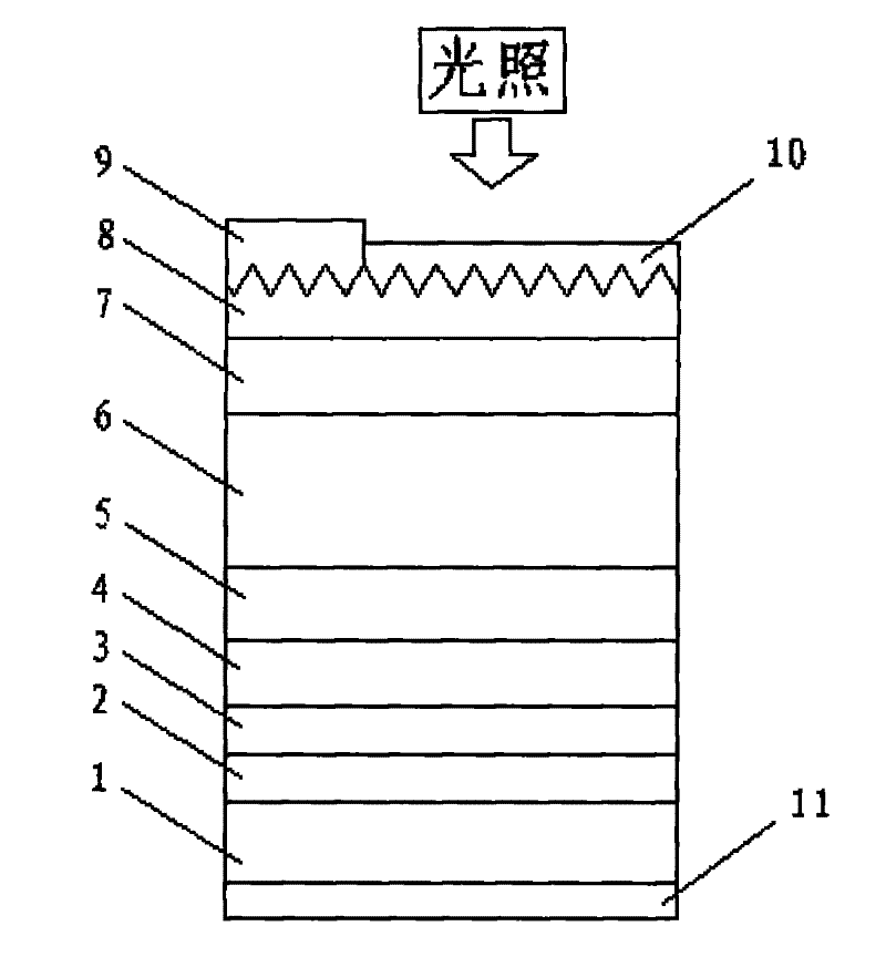
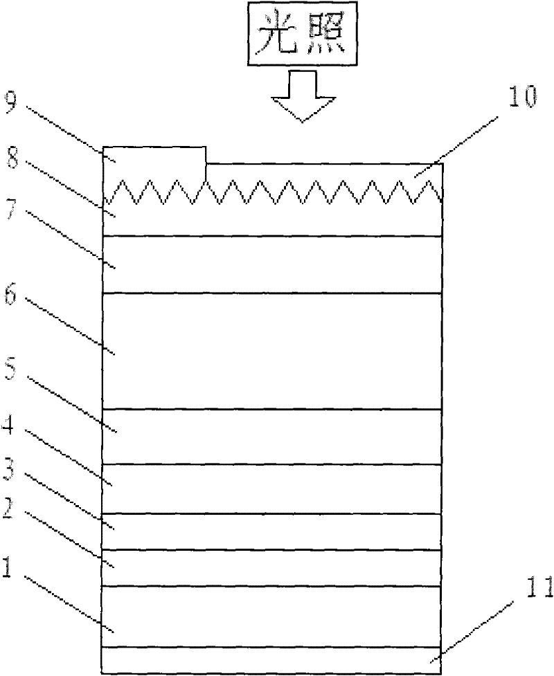
[0020] The structure of the solar cell is as figure 1 As shown: an n-type doped silicon substrate 1 is provided, and a layer of zinc oxide seed crystal layer 2 is formed on the silicon substrate. A zinc oxide nano-array buffer layer 3 is provided, which is fabricated on the zinc oxide seed crystal layer 2 . A layer of n-type doped gallium nitride buffer layer 4 is provided on the zinc oxide nano-array buffer layer 3 . With a layer of n-type doped In a Ga 1-a The N layer is made on the n-type doped gallium nitride buffer layer 3 . With a layer of unintentionally doped In b Ga 1-b N-layer 6, which is fabricated on n-type doped In a Ga 1-a N layer 5 above. with a layer of p-doped In c Ga 1-c N-layer 7, which is fabricated on unintentionally doped In b Ga 1-b N layer above. There is a layer of p-type heavily doped GaN window layer 8, which is fabricated on p-type doped I...
Embodiment 2
[0032] Example 2: Preparation of a silicon-based single-junction indium gallium nitride (InGaN) solar cell.
[0033] The preparation of the solar cell adopts the method comprising the following steps:
[0034] Step 1: Select an n-type doped silicon substrate 1, and obtain an n-type doped silicon wafer by doping phosphorus impurities;
[0035] Step 2: sputtering a 0.01-0.1 μm thick zinc oxide seed layer 2 on the surface of the silicon substrate, and then growing an aligned zinc oxide nano-array buffer layer 3 on the surface of the silicon wafer by wet chemical method, hydrothermal method or other methods , with a thickness of 0.2-2.5 μm.
[0036] Step 3: growing a silicon-doped n-type gallium nitride buffer layer 4 on the zinc oxide nano-array buffer layer 3 by using metal organic chemical vapor deposition technology. The growth temperature is 1000-1150°C, the growth pressure is 50-500torr, the thickness is 0.5-3μm, and the electron concentration is 1E16-1E19 / cm 3 ;
[0037...
PUM
 Abstract
Description
Claims
Application Information

