Display device
A technology for displaying data and displaying signals, which is applied in the field of current-driven display devices and can solve problems such as enlargement and problem increase
- Summary
- Abstract
- Description
- Claims
- Application Information
AI Technical Summary
Problems solved by technology
Method used
Image

Examples
Embodiment 1
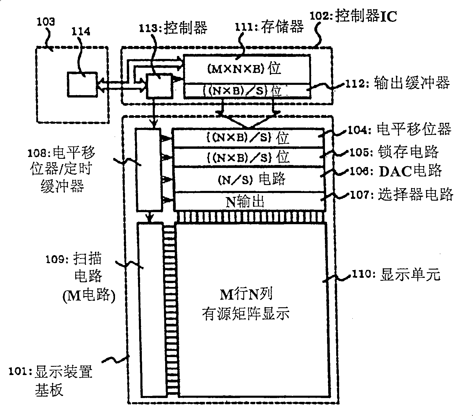
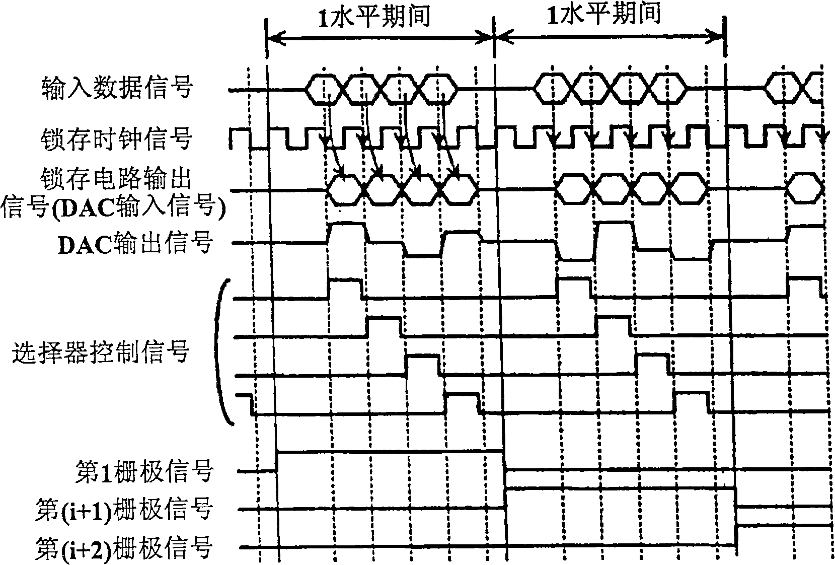
[0112] Fig. 1 shows a configuration diagram of a first embodiment of the present invention. A first embodiment of the present invention will be described in detail with reference to FIG. 1 . Referring to FIG. 1 , the first embodiment of the present invention is composed of a system-side circuit board 103 , a controller IC 102 , and a display device board 101 . The system circuit board 103 includes an interface circuit 114 and is connected to the controller IC 102 . The controller IC 102 includes a controller 113 , a memory 111 , and an output buffer 112 , and is connected to the system circuit board 103 and the display device board 101 . Display device substrate 101 is equipped with level shifter / timing buffer (controller) 106, scanning circuit (scanning line driving circuit) 109, level shifter 104, latch circuit 105, DAC circuit 106, selection circuit 107 and The display unit 110 is connected to the controller IC 102 . The level shifter circuit 104, the latch circuit 105, ...
Embodiment 2
[0134] Next, a second embodiment of the present invention will be described. Fig. 5 shows a configuration diagram of a second embodiment of the present invention. As shown in FIG. 5 , the second embodiment of the present invention is composed of a system-side circuit board 103 , a controller IC 102 , and a display device board 101 . The system circuit board 103 includes an interface circuit 114 and is connected to the controller IC 102 . The controller IC 102 includes a controller 113 , a memory 111 , and an output buffer 112 , and is connected to the system circuit board 103 and the display device board 101 . The display device substrate 101 is equipped with a level shifter / timing buffer 108, a scanning circuit 109, a level shifter 104, a latch circuit 105, a DAC circuit 106, a selector circuit 107, and a display unit 110, which are in phase with the controller IC 102. connect. The level shifter circuit 104 , the latch circuit 105 , the DAC circuit 106 , and the selector c...
Embodiment 3
[0138] Next, a third embodiment of the present invention will be described. Fig. 6 is a block diagram showing a third embodiment of the present invention. In FIG. 6 , the third embodiment of the present invention is composed of a system side circuit board 103 , a controller IC 102 and a display device board 101 . The system circuit board 103 includes an interface circuit 114 and is connected to the controller IC 102 . The controller IC 102 includes a controller 113 , a memory 111 , and an output buffer 112 , and is connected to the system circuit board 103 and the display device board 101 . Display device substrate 101 is equipped with level shifter / timing buffer 108, scanning circuit 109, level shifter 104, latch circuit 105, DAC circuit 106, selector circuit 107 and display unit 110, and is connected with controller IC102 . The latch circuit 105 , the level shifter 104 , the DAC circuit 106 , and the selector circuit 107 are arranged in this order, and the selector circui...
PUM
 Abstract
Description
Claims
Application Information
 - R&D Engineer
- R&D Manager
- IP Professional
- Industry Leading Data Capabilities
- Powerful AI technology
- Patent DNA Extraction
Browse by: Latest US Patents, China's latest patents, Technical Efficacy Thesaurus, Application Domain, Technology Topic.
© 2024 PatSnap. All rights reserved.Legal|Privacy policy|Modern Slavery Act Transparency Statement|Sitemap