An integrated light emitting diode die/lens structure, and process for the preparation thereof

A technology of light-emitting diodes and integral structures, which is applied in the manufacture of semiconductor/solid-state devices, electric solid-state devices, semiconductor devices, etc., can solve problems such as cracking of lens materials, peeling off of lens materials and supporting structures, and reduced long-term reliability of LEDs, etc., to achieve The effect of ensuring long-term reliability

Inactive Publication Date: 2008-11-26
SHIN ETSU CHEM IND CO LTD
View PDF1 Cites 13 Cited by
  • Summary
  • Abstract
  • Description
  • Claims
  • Application Information

AI Technical Summary

Problems solved by technology

[0003] However, thus obtained as figure 2 The overall structure of the LED chip and lens shown in (C) has the following problem. When the reliability of heat resistance and light resistance is high in applications such as vehicles, it is found that the lens material and LED The stress at the interface of the support structure of the chip will cause the lens material to crack, or the problem of peeling between the lens material and the support structure will occur, and the long-term reliability of the LED will be reduced

Method used


Image

  • An integrated light emitting diode die/lens structure, and process for the preparation thereof
  • An integrated light emitting diode die/lens structure, and process for the preparation thereof
  • An integrated light emitting diode die/lens structure, and process for the preparation thereof

Examples


Embodiment 1~4

[0070] Prepare a liquid silicone rubber composition (at 25°C, viscosity 10Pa·s) according to the following steps:

[0071] [Chem 2]

[0072]

[0073] (where L=450)

[0074] In 100 parts of dimethyl polysiloxane whose two ends are blocked by vinyl dimethyl siloxy groups, add the following formula (ii)

[0075] [Chem 3]

[0076]

[0077] (where L=10, M=8)

[0078] The organohydrogenpolysiloxane represented by , so that the molar ratio of the SiH group to the vinyl group in the above-mentioned vinyl group-containing dimethylpolysiloxane (i) reaches 1.5, and then add 0.05 parts of chloroplatinic acid Octanol modified solution, stir well.

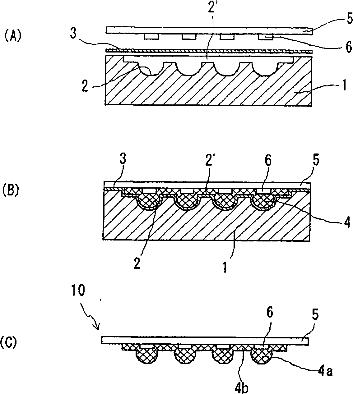
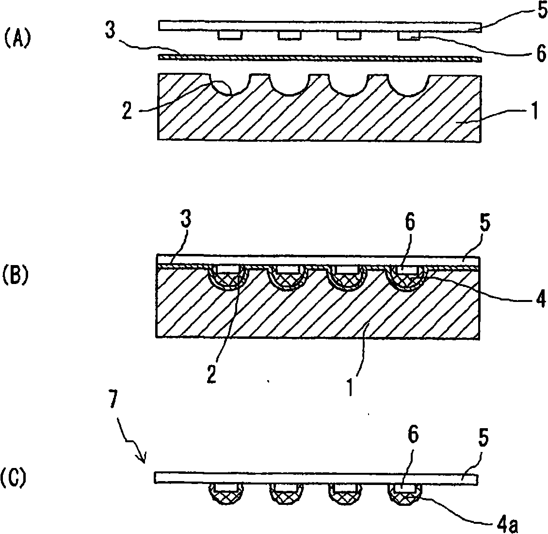
[0079] Next, a support structure in which 24 LED chips were mounted on an alumina substrate was prepared.

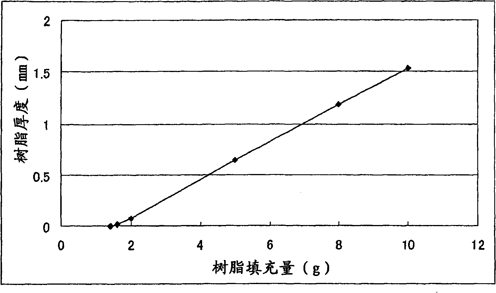
[0080] On the other hand, along figure 1 The concave mold cavity shown and the two mold cavities of the mold with a thickness of 0.01 to 2 mm are placed on the two mold cavities made by Nitto Denko Co., Ltd., and 1.8 g, 2.0g, 5...


PUM


Abstract

The invention provides an LED chip of a surface mounting type LED with high reliability and an integer structure of a lens and a manufacturing method thereof, characterized in that, through a middle layer of 0.01-2 mm thick, a convex lens part is formed on a supporting structure mounted with an LED chip; the LED chip mounted on the supporting structure is imbedded in the middle layer or imbedded from the middle layer to the convex lens part at the opposite position to the convex lens part, moreover, the middle layer and the convex lens part are made of the same materials to form an integer.

Description

technical field [0001] The present invention relates to an integral structure of light emitting diode (LED) chip and lens and its manufacturing method. Background technique [0002] It is well known that a lens is used on the LED chip to reduce the radiated light emitted by the LED chip or form a side radiation pattern. As a method of forming a lens for a surface-mounted LED, it is disclosed in JP-A-2006-148147 ( Patent document 1). The method, such as figure 2 As shown, on the mold 1 formed with the concave mold cavity 2 forming the convex lens part, the release sheet 3 is arranged along the concave mold cavity 2, and the liquid curable composition 4 is filled in the mold cavity 2 at the same time. The LED chip 6 installed on the support structure 5 is inserted into the curable composition 4 in the above-mentioned mold cavity 2, and after the curable composition 4 is cured, demoulding is carried out, and the molded object is removed from the mold cavity 2 of the mold 1. ...

Claims


Application Information

Patent Timeline
Patent Type & Authority Applications(China)
IPC IPC(8): H01L25/00H01L25/075H01L33/00H01L21/50H01L21/56H01L33/54H01L33/56
CPCH01L2224/97H01L2924/181H01L2924/00012
Inventor 今泽克之儿玉欣也柏木努
Owner SHIN ETSU CHEM IND CO LTD
Why Eureka
Try Eureka