Light-emitting device

一种发光装置、发射出的技术,应用在电气元件、电固体器件、电路等方向,能够解决接合线破裂、改变LED芯片发光特性等问题,达到降低线性膨胀系数的差异、减少组件或部件数、减少反射损失的效果

Inactive Publication Date: 2008-11-26
MATSUSHITA DENKO KK
View PDF1 Cites 17 Cited by
  • Summary
  • Abstract
  • Description
  • Claims
  • Application Information

AI Technical Summary

Problems solved by technology

The transmitted pressure may change the light-emitting characteristics of the LED chip and crack the bonding wire, or transfer external moisture to the LED chip

Method used


Image

  • Light-emitting device
  • Light-emitting device
  • Light-emitting device

Examples


no. 1 example

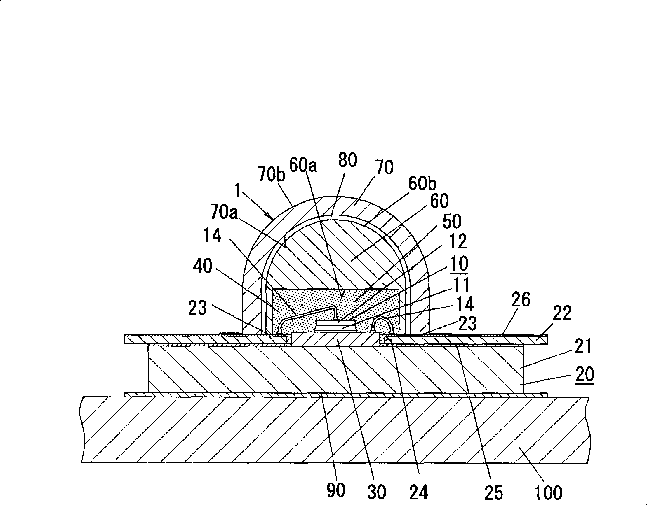
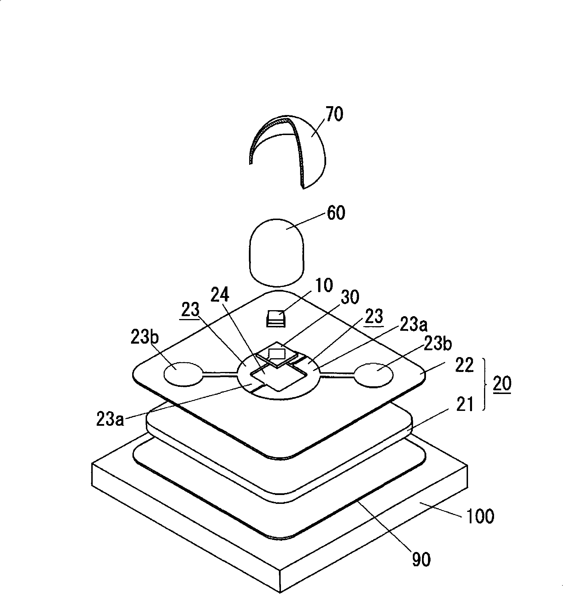
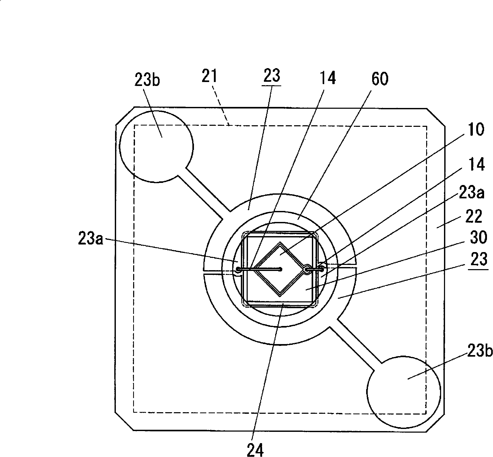
[0057] Such as Figure 1 to Figure 3 As shown, the light-emitting device 1 of this embodiment includes: LED chips 10; a mounting substrate 20 for mounting the LED chips 10; a packaging component 50, which has elasticity and is made of packaging resin materials, and is used to package the LED chips 10 and The bonding wire 14 connected to the LED chip 10 ; the lens 60 made of a transparent resin material; The color conversion component 70 is made of transparent material and fluorescent material; wherein, the fluorescent material is excited by the light emitted from the LED chip 10 to emit light of a color different from that emitted by the LED chip 10 . The lens 60 has a recess 40 facing the surface of the mounting substrate 20 ; and, by disposing the package component 50 in the recess 40 , the lens 60 is fixed on the mounting substrate 20 . The color conversion member 70 is arranged to cover the lens 60 such that an air layer 80 is formed between the color conversion member 70...

no. 2 example

[0087] The light emitting device 1 of the present embodiment consists of Figure 10 shown, and its basic components are almost identical to those of the first embodiment. Therefore, the same reference numerals are used to designate the same components, and related explanations will not be repeated.

[0088] In this embodiment, the inner diameter of the circular hole 26a formed in the central portion of the resist layer 26 is set to be slightly smaller than the maximum inner diameter of the color conversion member 70, and the color conversion member 70 is mounted on the mounting substrate through an adhesive 75 20, wherein the entire circumference of the color conversion member 70 is bonded to the periphery of the circular hole 26a.

[0089] The manufacturing method of the light emitting device 1 of this embodiment includes the following steps. First, the LED chip 10 is mounted on the mounting substrate 20, and the LED chip 10 is connected to the mounting substrate 20 through...

no. 3 example

[0092] The light emitting device 1 of the present embodiment consists of Figure 12 shown, and its basic components are almost identical to those of the first embodiment. Therefore, the same reference numerals are used to designate the same components, and related explanations will not be repeated.

[0093] In the present embodiment, the lens 60 is provided with: an injection port 41 for injecting the encapsulating resin material into the recess 40; and a discharge port 42 for discharging excess encapsulating resin material.

[0094] The manufacturing method of the light emitting device 1 in this embodiment includes the following steps. First, the LED chip 10 is mounted on the mounting substrate 20 , and the LED chip is connected to the mounting substrate 20 through the bonding wire 14 . Then, the lens 60 is adhered to the mounting substrate 20 to seat the LED chip 10 and the bonding wire 14 in the concave portion 40 of the lens (step (a)). Next, an uncured encapsulating resi...


PUM


Abstract

Disclosed is a light-emitting device (1) comprising an LED chip (10), a mounting board (20) on which the LED chip is mounted, a sealing portion (50) which is composed of a sealing resin material for sealing the LED chip, and a lens (60) made of a transparent resin material. The lens (60) has a recessed portion (40) in the bottom and is fixed to the mounting board (20) in such a manner that the sealing portion (50) is housed in the recessed portion (40). Since the sealing portion is surrounded by the transparent resin lens, the linear expansion coefficient difference between the sealing portion and the surrounding area thereof can be reduced in this light-emitting device. Consequently, there can be suppressed generation of voids in the sealing portion at low temperatures.

Description

technical field [0001] The present invention relates to a light emitting device using a light emitting diode (Light Emitting Diode, LED) chip and a manufacturing method thereof. Background technique [0002] Japanese Unexamined Patent Application Publication No. 2001-85748 (hereinafter referred to as Patent Document 1) and Japanese Unexamined Patent Application Publication No. 2001-148514 (hereinafter referred to as Patent Document 2) propose a light emitting device that emits The device includes an LED chip, a circuit board on which the LED chip is mounted, a metal support (for example, made of aluminum) surrounding the LED chip on the surface of the circuit board, and a metal frame filled in the support to package the LED chip and connect the LED chip. A package member for bonding wires (for example, made of transparent resin such as epoxy resin and silicone resin). The brackets disclosed in Patent Documents 1 and 2 have a shape having a notch that becomes larger as the d...

Claims


Application Information

Patent Timeline
Patent Type & Authority Applications(China)
IPC IPC(8): H01L33/00H01L33/32H01L33/50H01L33/56H01L33/58H01L33/62
CPCH01L2924/19107H01L33/52H01L33/58H01L2224/73265H01L2924/181H01L2924/00012
Inventor 桝井幹生浦野洋二
Owner MATSUSHITA DENKO KK
Why Eureka
Try Eureka