Optical sensor element, optical sensor device and image display device using optical sensor element

A technology for optical sensors and components, applied in electrical components, electrical solid-state devices, semiconductor devices, etc., can solve the problems of lower yield, many manufacturing processes, and difficulty in ensuring the flatness of components, so as to suppress the increase in process steps and maintain switching. characteristics, the effect of low noise characteristics

Inactive Publication Date: 2008-12-17
HITACHI LTD
View PDF6 Cites 6 Cited by
  • Summary
  • Abstract
  • Description
  • Claims
  • Application Information

AI Technical Summary

Problems solved by technology

However, this structure increases the sensor element formation process in the circuit formation process.
When forming such a multilayer structure, it is difficult to secure the flatness of the element, and it is difficult to secure sensor characteristics due to changes in optical characteristics
In addition, the yield may be lowered due to the large number of manufacturing processes

Method used


Image

  • Optical sensor element, optical sensor device and image display device using optical sensor element
  • Optical sensor element, optical sensor device and image display device using optical sensor element
  • Optical sensor element, optical sensor device and image display device using optical sensor element

Examples


Embodiment 1

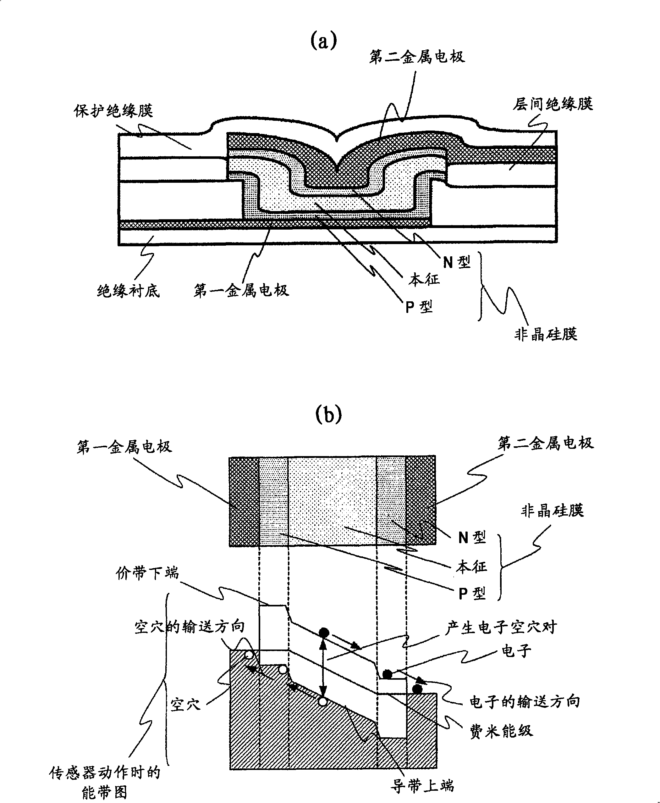
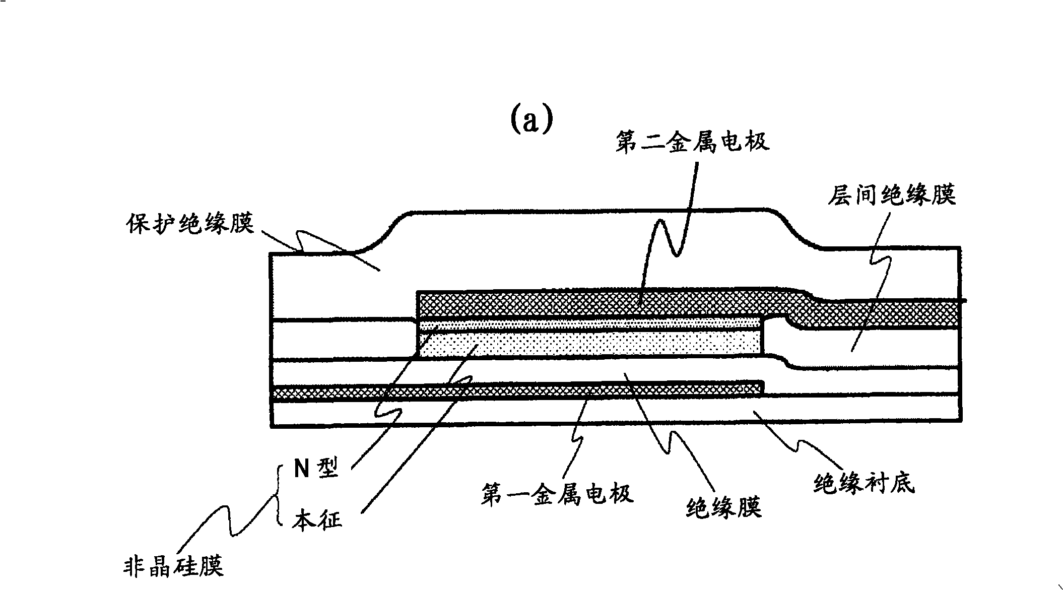
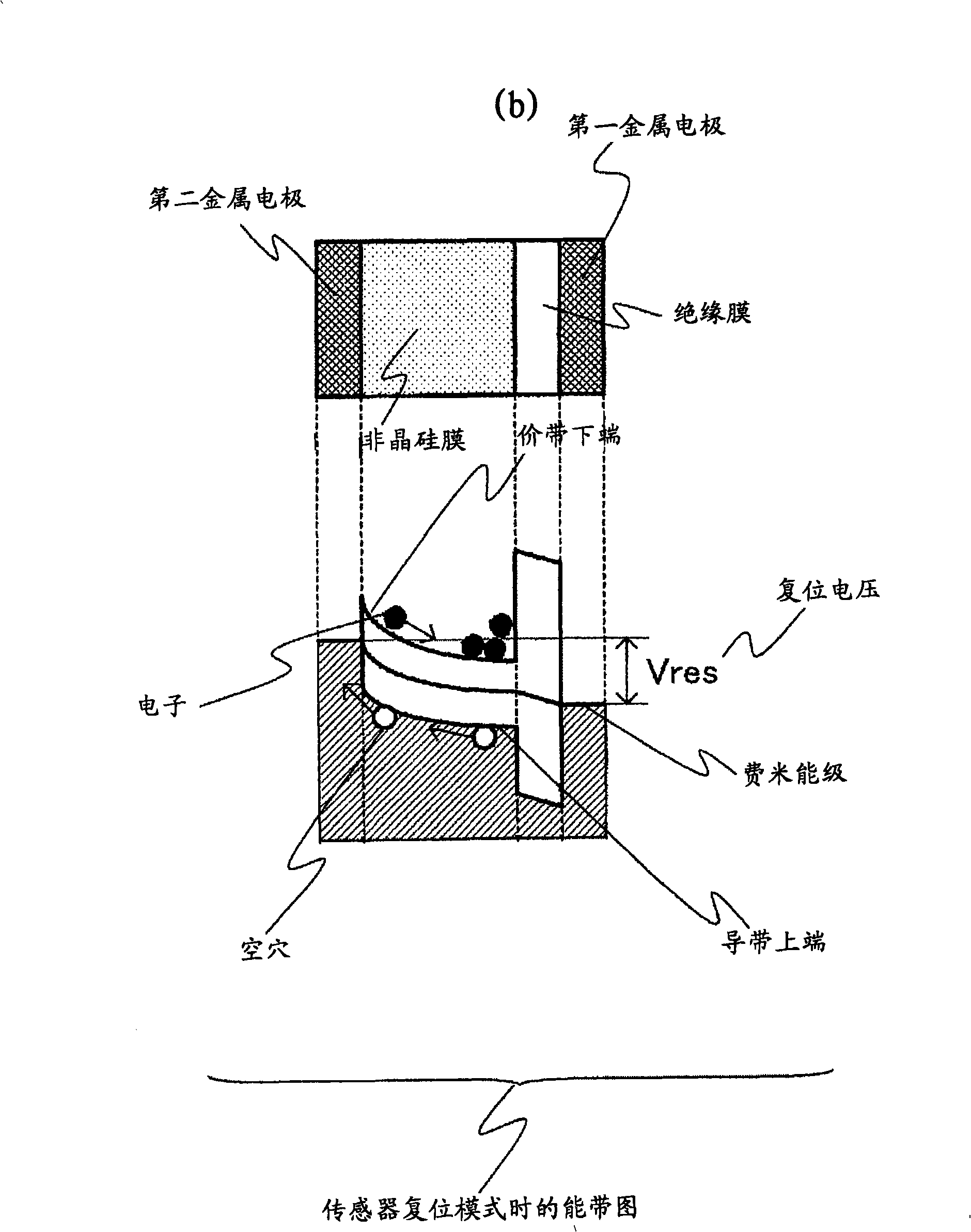
[0108] image 3 is a conceptual diagram of the photosensor element of the present invention. image 3 (a) is a cross-sectional view of an optical sensor element formed on an insulating substrate, image 3 (b) is a plan view.

[0109] exist image 3In this method, a polysilicon film is used to make a first electrode on an insulating substrate, a light-receiving layer is made of an amorphous silicon film thereon, and further, a first electrode transparent to visible light-near-infrared light is made through an insulating layer thereon. Two electrodes (the so-called transparent to visible light-near-infrared light mentioned here means that the energy transmittance for light with a wavelength of 400nm to 1000nm is more than 75%).

[0110] The first electrode is connected to the wiring layer through the contact hole. image 3 The example in fig. shows the case where the wiring layer is made of the same material as that of the second electrode, but it may be of a different mater...


PUM


Abstract

A highly sensitive optical sensor element, and a switch element such as a sensor driver circuit are formed on the same insulating substrate by using an LTPS planar process to provide a low cost area sensor (optical sensor device) incorporating the sensor driver circuit and the like or an image display device incorporating the optical sensor element. As an optical sensor element structure, one electrode of the sensor element is manufactured with the same film of the polycrystalline silicon film that is an active layer of the switch element constituting a circuit. A photoelectric conversion unit for performing photoelectric conversion is made of an amorphous silicon or a polycrystalline silicon film of an intrinsic layer. A structure in which the amorphous silicon of the photoelectric conversion unit and the insulating layer are sandwiched between two electrodes of the sensor element is adopted.

Description

technical field [0001] The present invention relates to a thin-film optical sensor element formed on an insulating film substrate and an optical sensor device using the element, in particular to an optical sensor array of an X-ray imaging device, a near-infrared detection device for biometric identification, or an optical sensor array on a display panel. Image display devices such as liquid crystal displays, organic EL (Electro Luminescence: electroluminescence) displays, inorganic EL displays, EC (Electro Chromic: electrochromic ) Low-temperature process semiconductor thin film transistors, low-temperature process photoconductive components or low-temperature process photodiode components used in displays. Background technique [0002] An X-ray imaging device is indispensable as a medical device, and the simplification of the operation of the device and the reduction of the cost of the device have always been problems to be solved. Furthermore, finger vein and palm vein re...

Claims


Application Information

Patent Timeline
Patent Type & Authority Applications(China)
IPC IPC(8): H01L31/09H01L31/0224H01L27/144
CPCH01L27/14609H01L27/14676H01L27/14692H01L31/03762H01L31/115Y02E10/548H01L31/12
Inventor 田井光春木下将嘉
Owner HITACHI LTD
Why Eureka
Try Eureka