
Non-volatile sequent modular memory, data storage and reading method

A technology for data storage and data storage, which is applied in the direction of static memory, read-only memory, digital memory information, etc., can solve the problems of high power consumption, slow speed, low repeatable reading and writing times, etc., so as to improve the reading and writing speed and reduce the The effect of power consumption

Inactive Publication Date: 2008-12-24
SHANGHAI INST OF MICROSYSTEM & INFORMATION TECH CHINESE ACAD OF SCI
View PDF0 Cites 9 Cited by
  • Summary
  • Abstract
  • Description
  • Claims
  • Application Information

AI Technical Summary

Problems solved by technology

But for a large amount of data storage, the RAM-style read and write method often results in higher power consumption, slower speed and lower repeatable read and write times.

Method used


Image

  • Non-volatile sequent modular memory, data storage and reading method
  • Non-volatile sequent modular memory, data storage and reading method
  • Non-volatile sequent modular memory, data storage and reading method

Examples


Embodiment 1

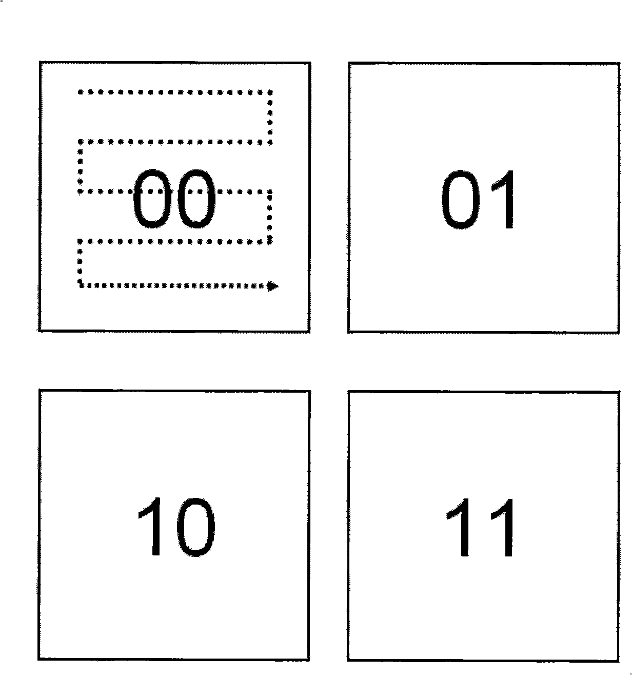
[0039] figure 1 A new type of non-volatile modular sequential memory is shown. First, the memory is divided, and each memory block is given a common address, and each memory block has only one address. The random reading and writing method is adopted between the storage blocks, and the sequential reading and writing method is adopted inside the storage block.

[0040] The storage method is as follows:

[0041] A11. The data to be stored points to a storage block.

[0042] A12. Store data in order.

[0043] A13. Complete the storage data operation.

[0044] The readout method is as follows:

[0045] B11. Find the storage data address

[0046] B12. Read out the data sequentially.

[0047] B13. Complete the data readout operation.

Embodiment 2

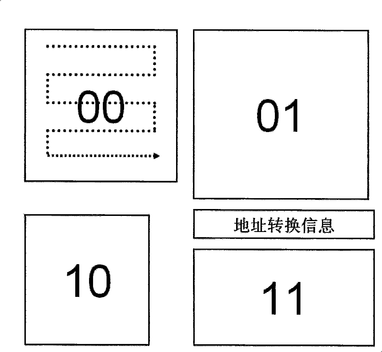
[0049] figure 2 An alternative to non-volatile block-style sequential storage is shown. Pre-evaluate the amount of data to be written, store data with a large amount of data in a storage block with a large capacity, and store data with a small amount of data in a storage block with a small capacity. This method should be divided into different sizes for the memory chip. Each memory block is marked with an address. In the process of storing data, first evaluate the amount of data to be stored. If the amount of data reaches a certain value, the address of the data is automatically converted to a specific storage block, and the conversion information is recorded in another non-volatile block. in the permanent storage block. In the readout process, the address conversion information is read out first, and then the data is read out according to the address conversion information.

[0050] The storage method is as follows:

[0051] A21. Evaluate the data to be stored.

[0052...

Embodiment 3

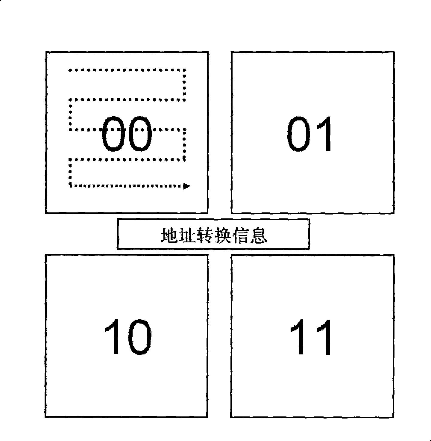
[0061] image 3 An alternative to non-volatile block-style sequential storage is shown. Pre-evaluate the amount of data to be written, and if the amount of data is large, divide and store the amount of data into two or more different storage blocks. In the process of storing data, firstly evaluate the amount of data to be stored. If the amount of data reaches a certain value, the data amount is divided and stored, and the address conversion information of the divided storage is stored in another non-volatile memory block. In the readout process, the address conversion information is read out first, and then the data is read out according to the address conversion information.

[0062] The storage method is as follows:

[0063] A31. Evaluate the data to be stored.

[0064] A32. If the amount of data is large, divide and store the amount of data into two or more different storage blocks. The address is converted into a suitable storage block, and the address conversion infor...


PUM


Abstract

The invention discloses a nonvolatile sequence module memory which is divided into a plurality of memory blocks. The data information of every memory block is assigned to a uniform address, a random writing and reading mode is adopted among all memory blocks and a sequence memory mode is adopted in the memory block. Aiming at a great deal of data memory, the memory of the invention changes the disadvantages of an RAM memory mode and proposes a set of novel nonvolatile sequence module memory and a memory and writing and reading method, thereby being capable of improving the writing and reading speed of a phase-change memory chip and writing and reading repetition times and reducing power consumption.

Description

technical field [0001] The invention belongs to the technical field of semiconductor storage, and relates to a memory, in particular to a non-volatile sequential modular memory; in addition, the present invention also relates to a data storage method and a data reading method of the non-volatile sequential modular memory. Background technique [0002] Phase change memory technology is based on Ovshinsky's proposal in the late 1960s (Phys. Rev. Lett., 21, 1450-1453, 1968) and early 1970s (Appl. Phys. Lett., 18, 254-257, 1971) The idea that the phase change film can be applied to the phase change storage medium is established, and it is a storage device with low price and stable performance. Phase-change memory can be made on a silicon wafer substrate, and its key materials are recordable phase-change films, heating electrode materials, heat-insulating materials, and lead-out electrode materials. Including how to reduce device material and so on. The basic principle of phase...

Claims


Application Information

Patent Timeline
IPC IPC(8): G11C11/56G11C16/08
Inventor 丁晟宋志棠陈邦明刘波陈小刚蔡道林封松林
Owner SHANGHAI INST OF MICROSYSTEM & INFORMATION TECH CHINESE ACAD OF SCI
Learn More