Semiconductor package and manufacturing method thereof

A semiconductor and packaging technology, applied in the field of semiconductor packaging and its manufacturing method, can solve the problems of high cost and complicated manufacturing process, and achieve the effects of reducing electrical connection paths, improving circuit layout and electrical connection quality

Inactive Publication Date: 2008-12-31
SILICONWARE PRECISION IND CO LTD
View PDF6 Cites 4 Cited by
  • Summary
  • Abstract
  • Description
  • Claims
  • Application Information

AI Technical Summary

Problems solved by technology

[0012] Another object of the present invention is to provide a semiconductor package and its manufacturing method, which can avoid the steps of using a dielectric layer, sputtering, electroplating, exposure, development and etching in the process of forming a circuit redistribution layer in the prior art. , leading to problems such as complicated manufacturing process and high cost

Method used


Image

  • Semiconductor package and manufacturing method thereof
  • Semiconductor package and manufacturing method thereof
  • Semiconductor package and manufacturing method thereof

Examples


no. 1 example

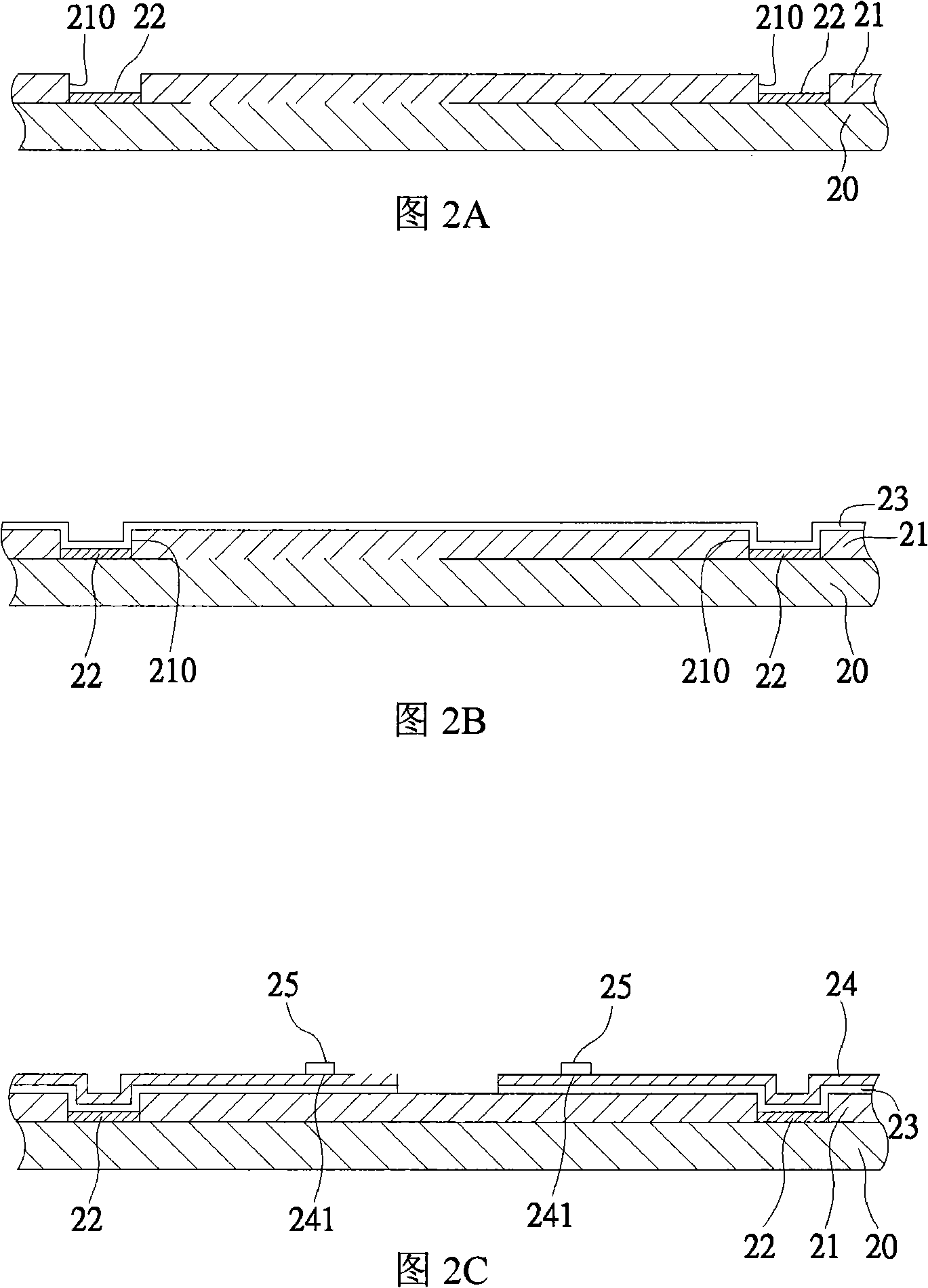
[0076] see Figure 3A to Figure 3F , is a schematic view of the first embodiment of the semiconductor package and its manufacturing method of the present invention.

[0077] Such as Figure 3A As shown, at first, prepare a carrier plate 30 of a metal material, such as a copper plate (CuPlate), and cover a first resistance layer 31 on a surface of the metal carrier plate 30, and make the first resistance layer 31 formed with a plurality of The first opening 310 is used to define a subsequent extension line for electrical connection with the semiconductor chip.

[0078] Then, an electroplating process is performed to form a metal block 32 in the first opening 310 by electroplating. The material of the metal block 32 is, for example, copper.

[0079] Such as Figure 3B and Figure 3C shown, where the Figure 3C for correspondence Figure 3B , then remove the first resistance layer 31, and cover the second resistance layer 33 on the metal carrier 30, and make the second resi...

no. 2 example

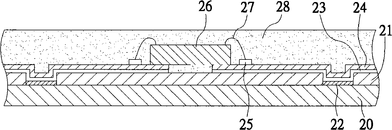
[0091] see again Figure 4 , is a schematic diagram of a second embodiment of the semiconductor package and its manufacturing method of the present invention.

[0092] The semiconductor package of this embodiment and its manufacturing method are substantially the same as those of the preceding embodiments, the main difference is that the insulating layer 48 can be filled in the groove 470 of the encapsulant 47 by, for example, dispensing, so as to cover and protect the grooves formed on the semiconductor package. The extension circuit 440 in the groove 470 is protected from external pollution or damage.

no. 3 example

[0094] see again Figure 5, is a bottom view of the third embodiment of the semiconductor package and its manufacturing method of the present invention.

[0095] The semiconductor package and its manufacturing method of this embodiment are substantially the same as those of the foregoing embodiments, the main difference being that the surface of the encapsulant 57 is formed with a plurality of grooves 570, and guide grooves 59 for connecting the grooves 570 are provided for convenience. The insulating layer 58 is filled in the groove 570 and the guide trench 59 by means of dispensing glue.


PUM


Abstract

The invention discloses an encapsulating piece of a semiconductor and a preparation method thereof. The invention provides a carrier plate on which a plurality of metal blocks are formed; a resistance layer is covered on the carrier plate and an opening which exposes the metal blocks are formed on the resistance layer, wherein, the width of the opening of the resistance layer is slightly smaller than that of the metal block so as to form a metal layer in the opening of the resistance layer; the metal layer comprises an extension circuit and an extension cushion and a welding cushion which are formed at an end point of the extension circuit; then the resistance layer is removed, and at least one semiconductor chip is electrically connected with the welding cushion, and an encapsulating glue body coating the semiconductor chip is formed on the carrier plate; then, the carrier plate and the metal blocks are removed to expose the metal layer so as to electrically connect the metal layer with external devices through interval conductive materials of the extension cushion of the exposed metal layer, therefore, the extension circuit can be flexibly arranged due to the integration degree of the chip so as to effectively reduce the electric connection path between the chip and the extension circuit.

Description

technical field [0001] The invention relates to a semiconductor package and its manufacturing method, in particular to a semiconductor package without a carrier and its manufacturing method. Background technique [0002] There are many types and types of traditional semiconductor packages that use lead frames as chip carriers. As far as Quad Flat Non-leaded (QFN) semiconductor packages are concerned, they are characterized in that no external leads are provided. That is, there is no external pin for electrical connection with the outside as in the existing quad flatpackage (QFP) semiconductor package, so that the size of the semiconductor package can be reduced. [0003] However, with the development trend of thinner and smaller semiconductor products, the traditional QFN package with lead frame is often unable to further reduce the overall height of the package due to the limitation of the thickness of the encapsulant. Therefore, the industry has developed a carrierless (ca...

Claims


Application Information

Patent Timeline
Patent Type & Authority Applications(China)
IPC IPC(8): H01L21/50H01L21/60H01L21/56H01L23/488H01L23/31
CPCH01L2224/48091H01L2924/15311H01L2924/00014
Inventor 李春源黄建屏江连成徐维宏王智祥
Owner SILICONWARE PRECISION IND CO LTD
Why Eureka
Try Eureka