Semiconductor packaging member and method for fabricating the same

A semiconductor and packaging technology, applied in the field of semiconductor packaging and its manufacturing method, can solve problems such as the reliability of solder joint cracks, shorten the arc length of welding wires, and reduce fatigue life, so as to improve circuit layout and electrical connection quality, shortening the electrical connection path, and shortening the arc length of the welding wire

Inactive Publication Date: 2008-06-04
SILICONWARE PRECISION IND CO LTD
View PDF2 Cites 21 Cited by
  • Summary
  • Abstract
  • Description
  • Claims
  • Application Information

AI Technical Summary

Problems solved by technology

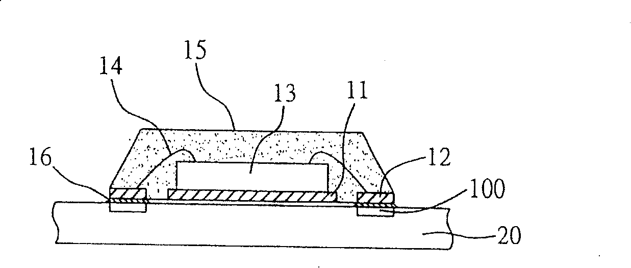
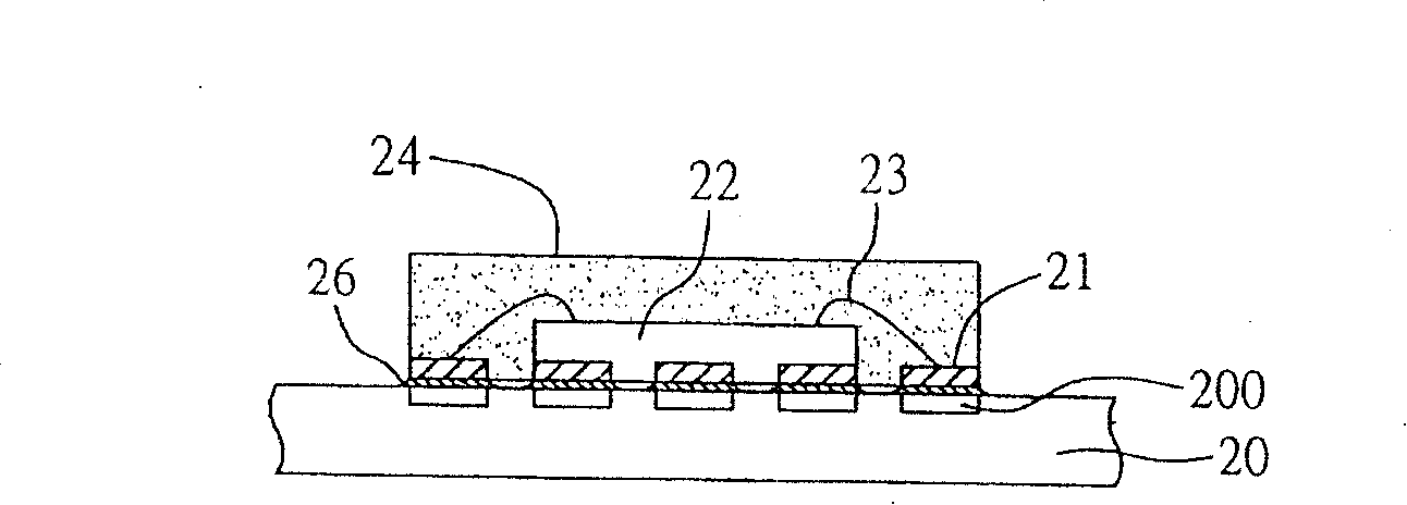
Therefore, in the aforementioned existing semiconductor package, due to the extremely low height of the solder joint, a great thermal stress will be generated on the solder joint between the semiconductor package and the printed circuit board, which not only causes the semiconductor package The fatigue life of the solder joints with the printed circuit board is reduced, which will even cause cracks in the solder joints, seriously affecting the reliability of electronic products; relatively, if the setting and height of the solder volume are increased, Also, due to the excessive amount of solder, or poor control of the contact distance between the package and the printed circuit board, the adjacent solder material contacts and a short circuit occurs, which leads to troubles in the manufacturing method.
[0010] Therefore, how to solve the above problems and provide a semiconductor package without a carrier and its manufacturing method, avoid cracks and poor reliability of solder joints, and flexibly arrange circuits to effectively shorten the welding line Arc length, so as to improve the circuit layout and electrical connection quality, it is urgent

Method used


Image

  • Semiconductor packaging member and method for fabricating the same
  • Semiconductor packaging member and method for fabricating the same
  • Semiconductor packaging member and method for fabricating the same

Examples


no. 1 example

[0072] see Figures 4A to 4G , is a schematic cross-sectional view of the first embodiment of the semiconductor package and its manufacturing method of the present invention.

[0073] Such as Figure 4A As shown, at first, a metal carrier (Carrier) 40 such as a copper plate (Cu Plate) is prepared, and a sacrificial layer 41 is laid on one surface of the metal carrier 40, and the sacrificial layer 41 is, for example, polymer (polymer) It is made of materials, such as epoxy, photo-resist, etc., and its thickness is about 10 to 30 μm. The sacrificial layer 41 is formed by conventional methods of coating, exposure, development and etching, or by stencil printing to form the sacrificial layer 41 with a plurality of through openings 410 .

[0074] Such as Figure 4B As shown, an insulating layer 42 is laid on the surface of the sacrificial layer 41, and the insulating layer 42 is, for example, a solder mask (Solder Mask), and the insulating layer 42 is exposed by conventional coa...

no. 2 example

[0083] see Figure 5A and 5B , is a cross-sectional view of the second embodiment of the semiconductor package of the present invention. Such as Figure 5A As shown, the semiconductor package of this embodiment is roughly the same as the previous embodiment, the main difference is that the chip 58 of this embodiment is connected to the patterned circuit layer 55 in a flip-chip method (Flip-Chip); In other words, during the die bonding operation, the active surface of the chip 58 faces the patterned circuit layer 55 and is electrically connected to the terminal 550 of the patterned circuit layer 55 or the metal on the terminal 550 through a plurality of solder bumps 54 . layer 56 , and then form an encapsulant 59 covering the chip 58 . Compared with connecting the chip and the patterned circuit layer with bonding wires, the flip-chip technology using solder bumps can further shorten the electrical connection path between the chip and the patterned circuit layer, and can bett...


PUM


Abstract

The invention relates to an encapsulation piece of a semiconductor and a manufacturing method thereof. The method essentially includes the following steps: a sacrificial layer is laid between a metallic carrier tool and an insulating layer, and preconcerted parts of the sacrificial layer and the insulating layer are opened with a plurality of perforative openings, so that a conductive metal layer can be generated in the openings subsequently and a patterned line layer can be generated on the insulating layer subsequently, and the patterned line layer is electrically connected with the conductive metal layer; then at least one chip is electrically connected with the patterned line layer and an encapsulated colloid which wraps the chip and the patterned line layer, in other words, the metallic carrier tool and the sacrificial layer are removed, so that the conductive metal layer generated formerly to prong the sacrificial layer and the opening of the insulating layer is relatively protruded when compared with the insulating layer; in this way, when the completed encapsulation piece of the semiconductor is electrically connected with outer devices, a distance between the encapsulation piece of the semiconductor and the outer devices can be increased, as a result, thermal stress generated by difference of thermal expansion coefficient between the encapsulation piece of the semiconductor and the outer devices can be reduced, and the reliability is improved.

Description

technical field [0001] The invention relates to a semiconductor package and its manufacturing method, in particular to a semiconductor package that does not need a carrier and its manufacturing method. Background technique [0002] Traditional semiconductor chips use a lead frame as a chip carrier to form a semiconductor package. The welding frame includes a chip holder and a plurality of leads formed around the chip holder. After the semiconductor chip is bonded to the chip holder and the chip and the leads are electrically connected by welding wires, the chip is covered by encapsulation resin, The chip base, the bonding wire and the inner section of the lead form the semiconductor package with the soldering frame. [0003] There are many types and types of semiconductor packages with soldering frames as chip carriers. As far as the quad flat non-leaded (QFN) semiconductor package is concerned, it is characterized in that no external leads are provided. That is, there is ...

Claims


Application Information

Patent Timeline
Patent Type & Authority Applications(China)
IPC IPC(8): H01L21/50H01L21/60H01L23/498H01L23/488
CPCH01L2224/48091H01L2224/16H01L2224/48247H01L2924/00014
Inventor 姜亦震普翰屏黄建屏萧承旭
Owner SILICONWARE PRECISION IND CO LTD
Why Eureka
Try Eureka