Surface roughness recognizing and classifying method for LED chip

A technology of LED chip and surface roughness, which is applied in the field of identification and classification of the surface roughness of LED chips, can solve the problems of LED chip positioning operation troubles and other problems, achieve uniform brightness and avoid the effect of misoperation

Active Publication Date: 2008-12-31
EPILIGHT TECH
View PDF0 Cites 7 Cited by
  • Summary
  • Abstract
  • Description
  • Claims
  • Application Information

AI Technical Summary

Problems solved by technology

The automated microscope machine will treat the darker LED chip as the background and cannot be recognized, or it will shut down if it thinks it is not the

Method used


Image

  • Surface roughness recognizing and classifying method for LED chip

Examples


Embodiment Construction

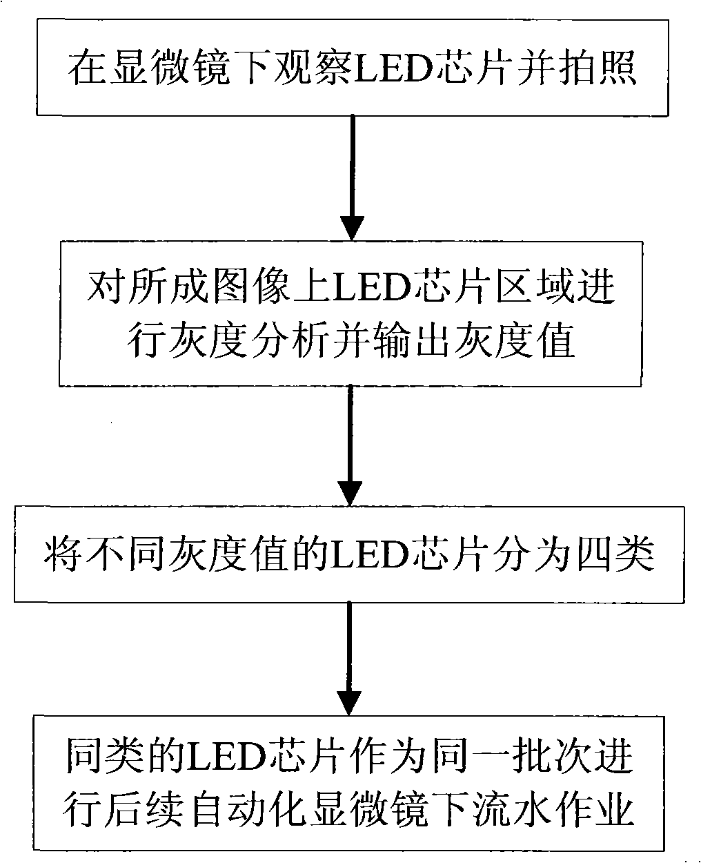
[0013] The identification and classification method of the LED chip surface roughness of the present invention is accomplished by a microscope and a grayscale identification system. figure 1 Be the flow chart of the present invention, introduce the step of the present invention in detail below:

[0014] Step 1: First put the gallium nitride-based LED chip under the microscope, the magnification is 10 times, and the magnification of the automatic microscope machine usually used for production is the same. At this time, an area with a certain brightness observed under the microscope is the position of the LED chip. LED chips with different surface roughness show different brightness under the microscope. Then use the CC integrated with the microscope to take pictures of the microscope image and save it.

[0015] Step 2: Use the grayscale recognition system to carry out grayscale recognition on the P electrode area and N electrode area of ​​the LED chip on the image saved in th...


PUM


Abstract

The invention discloses an identification and classification method for the roughness of LED chip surfaces; the method includes the following steps: (1) the LED chip is put under a microscope to observe p electrode area and N electrode area in the LED ship and the microscopic images are photographed; (2) a gray scale identification system is utilized to identify the gray scale for the P electrode area and N electrode area of the LED chip in the microscopic images and the value of gray scale is output; (3) the observed LED chips are classified into four types; (4) when an operation under microscope is necessary, LED chips of the same types classified according to the step (3) are deemed as the same batch and operated in the way of line production. According to the classification method of the invention, classified LED chips can be easily recognized when the chips are under automatic microscopic operation. The classification method of the invention can be used for the classification of LED chips of different surface roughness.

Description

technical field [0001] The invention relates to a method for identifying and classifying the surface roughness of an LED chip, in particular to a method for identifying and classifying the roughness of a gallium nitride-based LED chip. Background technique [0002] Due to its special physical and chemical properties, semiconductor light-emitting diodes (LEDs) have the following advantages: high efficiency and energy saving, power consumption is one-eighth of incandescent lamps, and one-half of fluorescent lamps; solid structure, can be used in harsh environments , with a service life of up to 100,000 hours, ten times higher than the current incandescent lamp; no mercury, chromium and other toxic heavy metal elements, easy to recycle, and realize true green lighting; simple structure, small size, light weight, fast response, and low working voltage , has the advantages of safety and earthquake resistance, and is internationally recognized as a new generation of light sources ...

Claims


Application Information

Patent Timeline
IPC IPC(8): H01L21/66G01B11/30
Inventor 姜森来梁国荣李智武
Owner EPILIGHT TECH
Why Eureka
Try Eureka