Printed circuit board, electronic member mounting method and electronic device

一种印刷线路板、电子设备的技术,应用在印刷电路零部件、印刷电路、印刷电路等方向,能够解决降低连接可靠性等问题,达到高密度安装连接可靠性的效果

Inactive Publication Date: 2008-12-31
KK TOSHIBA
View PDF1 Cites 7 Cited by
  • Summary
  • Abstract
  • Description
  • Claims
  • Application Information

AI Technical Summary

Problems solved by technology

[0007] An object of the present invention is to provide a printed wiring board structure capable of high-density mounting and high-density wiring without reducing connection reliability

Method used


Image

  • Printed circuit board, electronic member mounting method and electronic device
  • Printed circuit board, electronic member mounting method and electronic device
  • Printed circuit board, electronic member mounting method and electronic device

Examples


Embodiment Construction

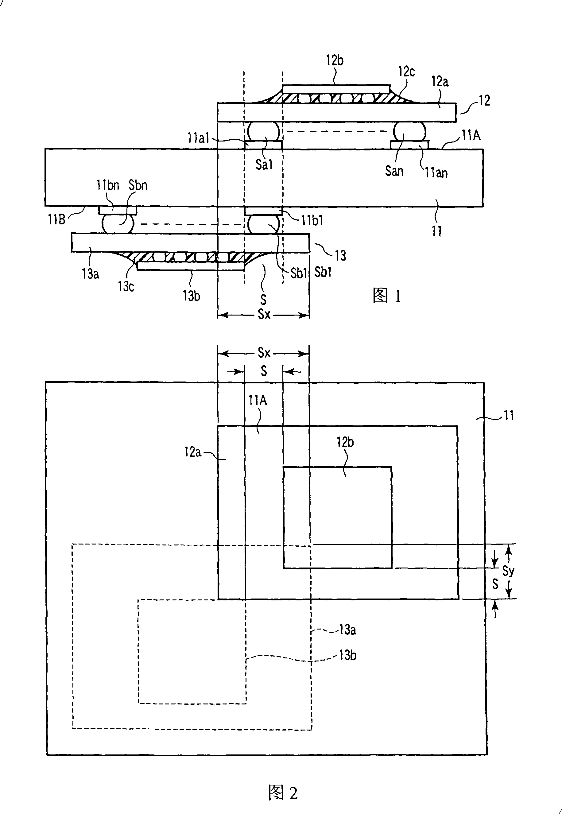
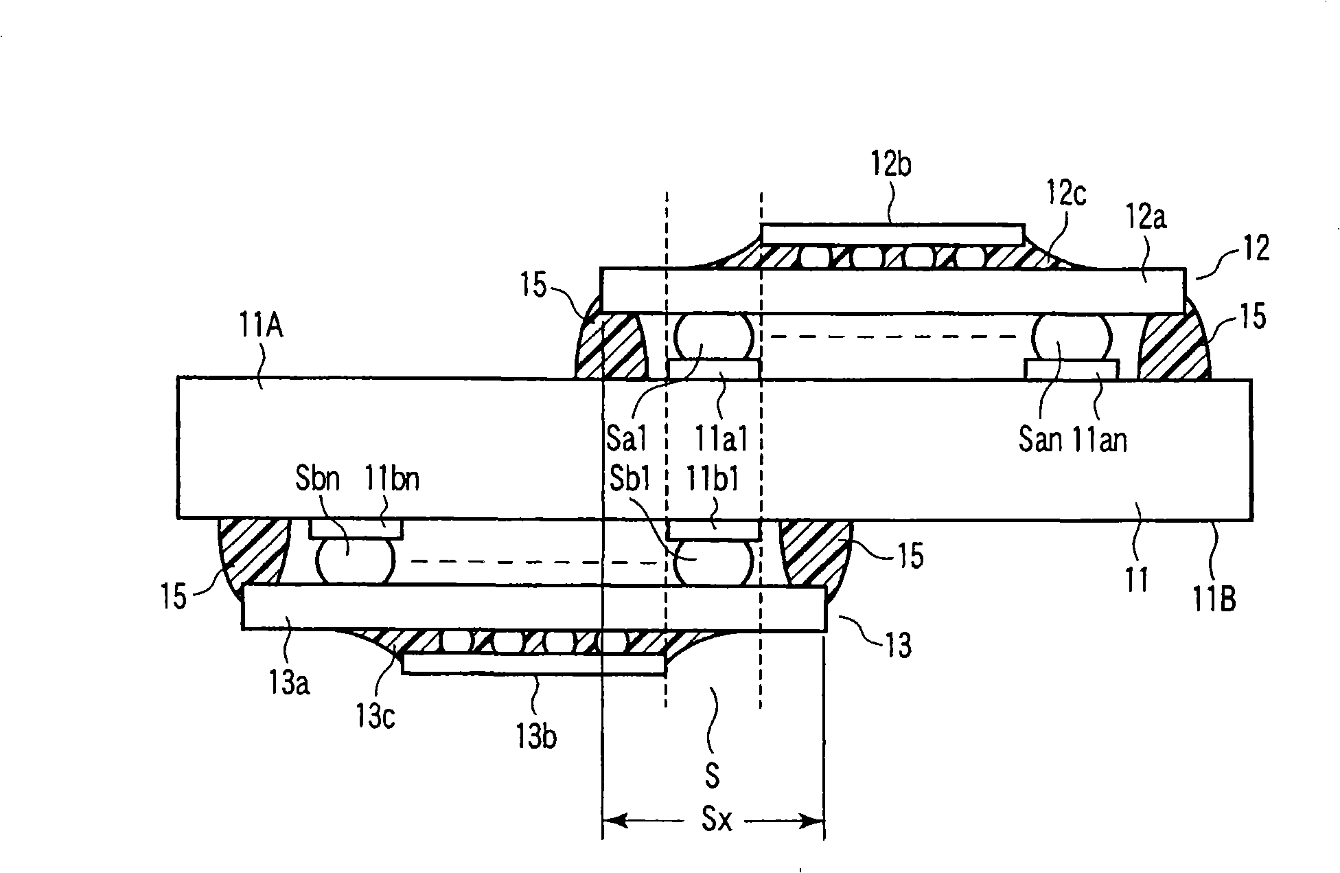
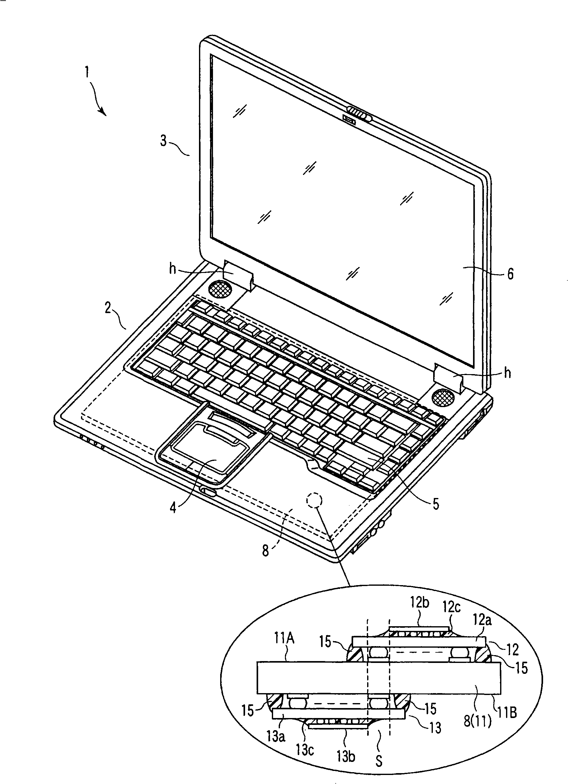
[0019] Hereinafter, various embodiments according to the present invention will be described with reference to the accompanying drawings. Generally, according to an embodiment of the present invention, a printed circuit board structure is provided, including:

[0020] A printed wiring board having first and second component mounting surfaces at its front and rear sides, each of which is used to mount a semiconductor package as a mounted component, the semiconductor package being loaded on Semiconductor chips on substrates;

[0021] a first semiconductor package mounted on the first component mounting surface; and

[0022] a second semiconductor component mounted on the second component mounting surface,

[0023] Wherein the first and second semiconductor components have a positional relationship such that the substrates are partially overlapped via the printed wiring board and the semiconductor chips are not overlapped.

[0024] According to the printed wiring board structu...


PUM


Abstract

According to one embodiment, a printed wiring board structure comprises a printed wiring board having first and second component mounting surfaces at front and back sides thereof, respectively, each for mounting a semiconductor package loading a semiconductor chip loaded on a substrate as a mounting component, a first semiconductor package mounted on the first component mounting surface, and a second semiconductor package mounted on the second component mounting surface, wherein the first and second semiconductor packages have a positional relationship such that the substrates are partially overlapped via the printed wiring board, and the semiconductor chips are not overlapped.

Description

technical field [0001] One embodiment of the present invention relates to a printed wiring board structure in which semiconductor components having semiconductor chips mounted on a substrate are mounted on both sides of the printed wiring board. Background technique [0002] A circuit board, on which large semiconductor components forming a CPU and its peripheral circuits are mounted, is provided as a main component in a casing of an electronic device such as a personal computer. This large semiconductor component has tens of millimeters square. [0003] Such circuit boards for electronic equipment such as personal computers require means for protecting the mounting surfaces of semiconductor components. In particular, it is necessary to protect the mounting surface from bending and deformation of the substrate and from stress applied by external shocks and vibrations. [0004] For example, a method disclosed in Japanese Patent Application Laid-Open No. 2002-271014 has been...

Claims


Application Information

Patent Timeline
Patent Type & Authority Applications(China)
IPC IPC(8): H05K1/18H05K3/34
CPCH01L2224/73204H05K1/0271H05K1/181H05K3/305H05K2201/10545H05K2201/10734Y02P70/50
Inventor 泷泽稔
Owner KK TOSHIBA
Why Eureka
Try Eureka