Line forming method adopting printing means
A technology of circuit and means, applied in the direction of conductive pattern formation, can solve the problem of difficult to improve conductivity, and achieve the effect of no pollution and precise production
- Summary
- Abstract
- Description
- Claims
- Application Information
AI Technical Summary
Problems solved by technology
Method used
Image

Examples
Embodiment Construction
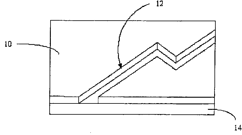
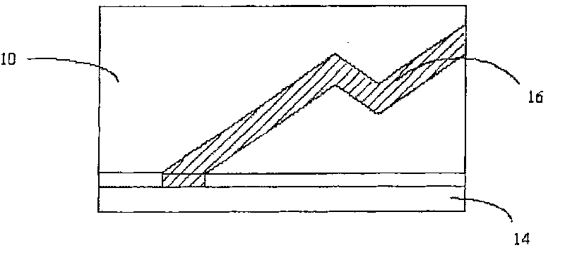
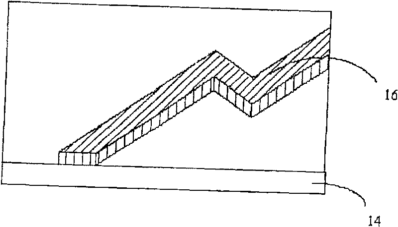
[0023] see Figure 1A-1D , Figure 1A-1D It is a schematic diagram of the circuit forming method using printing means in the present invention. Such as Figure 1A-1D As shown, the present invention mainly does not use etched copper foil to form lines, but uses such as Figure 1D The adhesive layer 16 shown adheres the metal powder and solidifies the metal powder to form the circuit 18 , so as to provide the convenience of coating like the conductive adhesive, but better than the conductive effect of the conductive adhesive.
[0024] In simple terms, the present invention is as follows Figure 1A A patterned screen 10 (having a traversing pattern 12 relative to a predetermined line), a substrate 14 is provided as shown, and as shown in FIG. Figure 1B As shown, the patterned screen 10 is used to transfer the adhesive to the substrate 14, and a patterned adhesive layer 16 is formed on the substrate 14, as shown in FIG. Figure 1C shown. Then, apply metal powder to the adhesiv...
PUM
 Abstract
Description
Claims
Application Information
PatSnap Eureka turns technology decisions into work you can execute. Powered by our Innovation Knowledge Graph, it runs expert workflows across engineering, life sciences, materials and intellectual property. Get your review-ready output in minutes.


