Integrated circuit structure for test

A technology of integrated circuits and test keys, which is applied to circuits, electrical components, and electrical solid-state devices, etc., can solve the problems of increased process costs, and the inability to improve the space utilization rate of the wafer's dicing lanes and manufacturing costs.

Inactive Publication Date: 2009-01-21
UNITED MICROELECTRONICS CORP
View PDF0 Cites 5 Cited by
  • Summary
  • Abstract
  • Description
  • Claims
  • Application Information

AI Technical Summary

Problems solved by technology

In this way, it will also cause a substantial increase in process costs
[0005] Therefore, it can be seen that due to the limitation of the current process technology, it is impossible to improve the

Method used


Image

  • Integrated circuit structure for test
  • Integrated circuit structure for test
  • Integrated circuit structure for test

Examples


Embodiment Construction

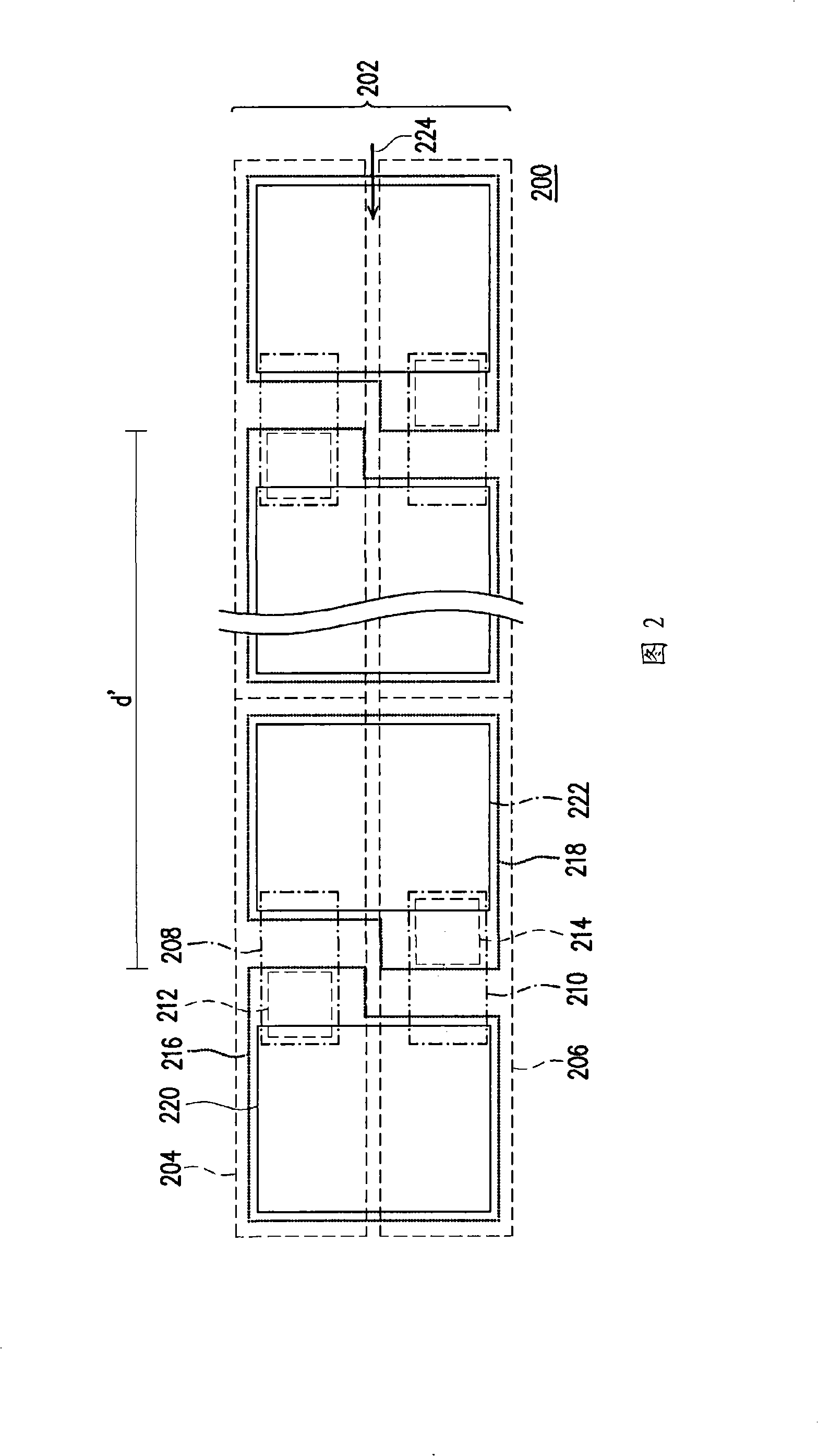
[0045] FIG. 2 is a top view of an integrated circuit structure for testing according to an embodiment of the present invention. In FIG. 2, the size and spacing of each component are all defined by current technology, and the present invention is not limited thereto.

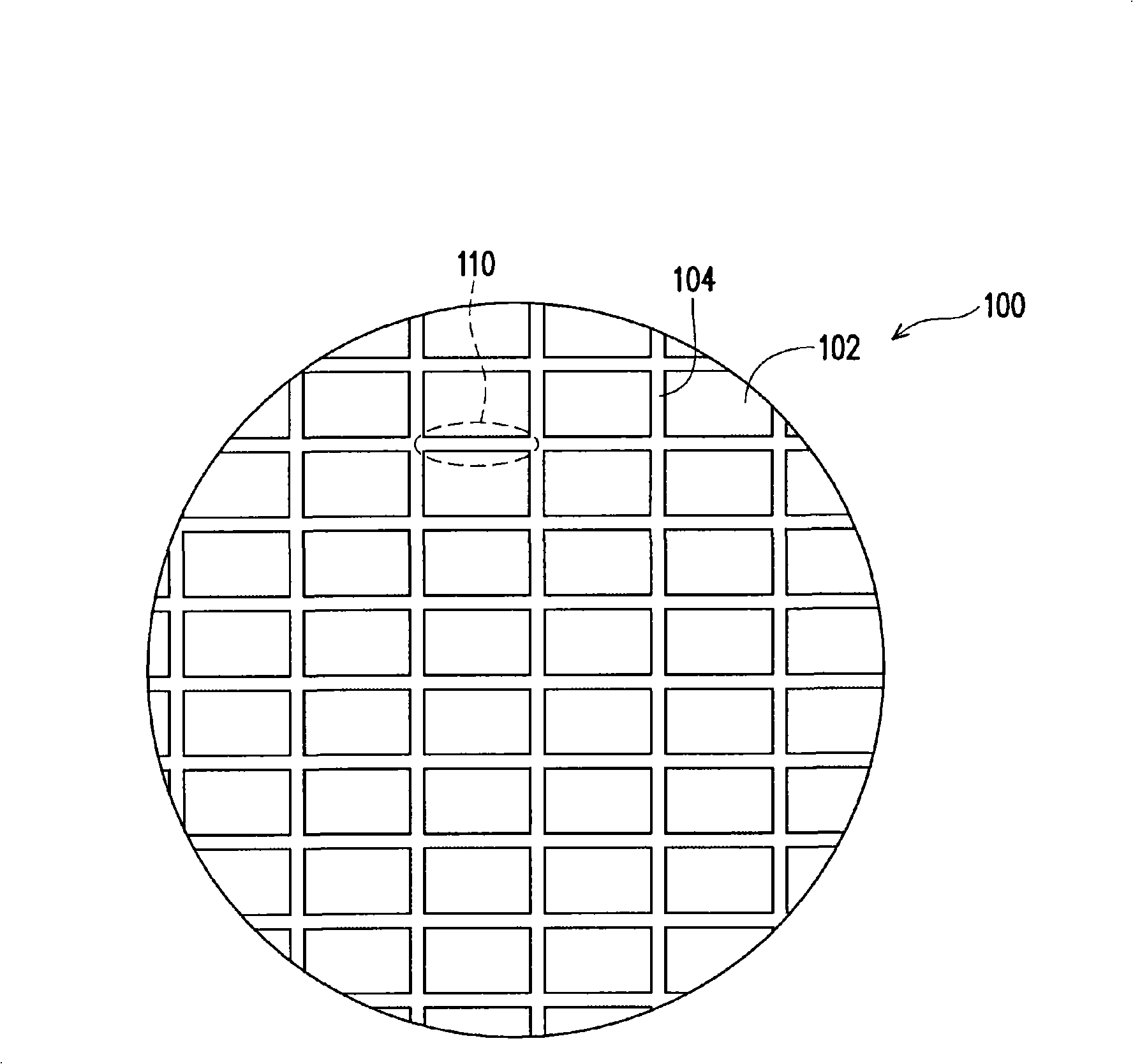
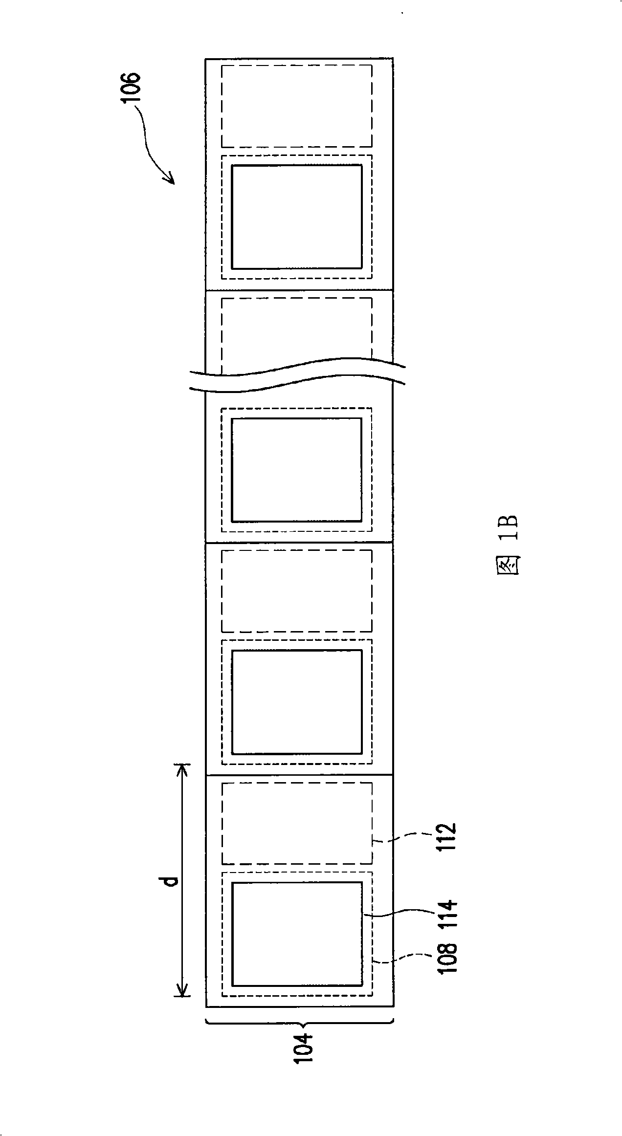
[0046] Please refer to FIG. 2, the wafer / substrate 200 has a device area (not shown) and a dicing channel area 202. Among them, the device area of ​​the wafer / substrate 200 refers to the area of ​​a die, which is a place where active circuit elements and interconnections are formed. The scribe area 202 refers to the area surrounding the die to separate the die. It will also be formed with similar active circuit components and interconnection structures at the same time, which is used as a test key for testing purposes. . Moreover, the manufacturing steps of active circuit elements and interconnections in the scribe zone 202 are generally integrated with the process of the element zone. The active circuit components o...


PUM


Abstract

The invention discloses an integrated circuit structure for testing, which is positioned in a cutting channel region and comprises a first/a second testing keys, a first/a second conducting electrical connectors, a first/a second testing welding pads and a protective layer, wherein the first/the second testing keys comprise a first/a second active circuit elements which are collocated in a substrate of the cutting channel region and a first/a second inner connecting wires which are electrically connected with the first/the second active circuit elements. The second testing key and the first testing key are basically arranged in parallel. The first/the second conducting electrical connectors are positioned on the first/the second inner connecting wires and are connected with the upmost metallic layer of the second inner connecting wire. The first/the second testing welding pads are collocated above the first and the second testing keys and are contacted with the first/the second conducting electrical connectors. The protective layer is provided with a first opening which exposes a part of the first/ the second testing welding pads and a second opening which exposes a part of the second welding pad.

Description

Technical field [0001] The present invention relates to an integrated circuit structure, and particularly relates to a test integrated circuit structure that can improve the space utilization rate of a cutting lane. Background technique [0002] After the wafer is manufactured and before dicing and packaging, a wafer acceptance testing (WAT) method is commonly used to measure the yield of semiconductor components on the wafer. In this method, around the die on the wafer, that is, on the wafer with multiple scribe lines that are parallel and perpendicular to each other, multiple test keys are specially provided. These test keys will then be electrically connected to external circuits or probes for probe cards through pads for testing, so as to monitor the quality of each stage of the process. Generally, the component structure generally formed on the die is mainly used to participate in logic operations or memory functions, and a similar component structure is also formed on the c...

Claims


Application Information

Patent Timeline
IPC IPC(8): H01L23/544
Inventor 郭建利吴炳昌
Owner UNITED MICROELECTRONICS CORP
Why Eureka
Try Eureka