Capacitor and manufacturing method thereof

A manufacturing method and capacitor technology, which is applied in semiconductor/solid-state device manufacturing, electric solid-state devices, circuits, etc., can solve problems such as high process temperature and process execution time, difficulty in integrating capacitors, and limited manufacturing space size

Inactive Publication Date: 2009-01-21
PROMOS TECH INC
View PDF0 Cites 0 Cited by
  • Summary
  • Abstract
  • Description
  • Claims
  • Application Information

AI Technical Summary

Problems solved by technology

[0005] However, the above-mentioned application technology of growing hemispherical dies of silicon materials usually requires extremely high process temperature and process execution time, and the size of the grown hemispherical dies is often limited by the size of the capacitor manufacturing space such as trenches. , so it is not easy to integrate in the fabrication of DRAM using capacitors placed in trenches

Method used


Image

  • Capacitor and manufacturing method thereof
  • Capacitor and manufacturing method thereof
  • Capacitor and manufacturing method thereof

Examples


Embodiment Construction

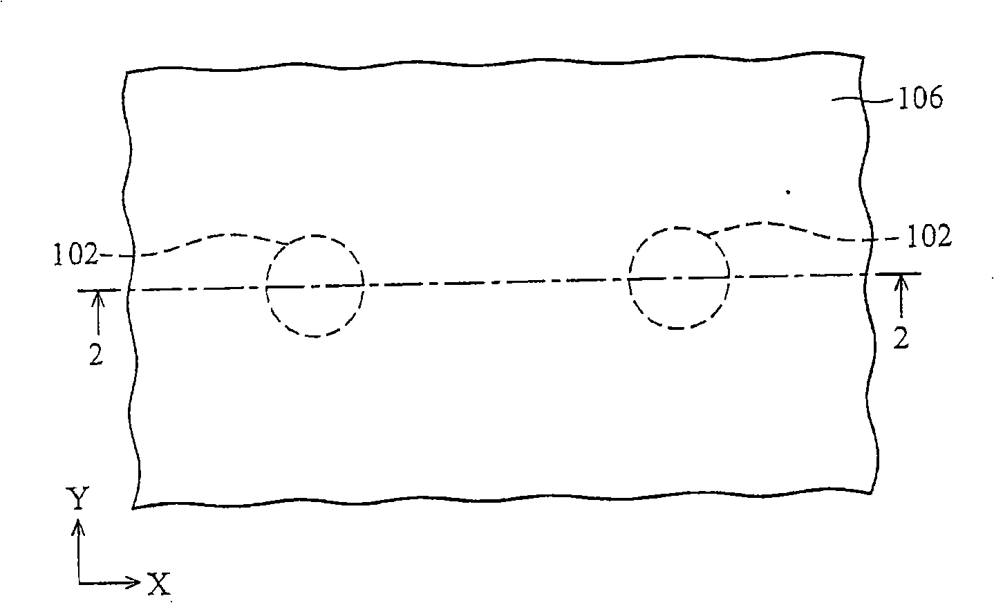
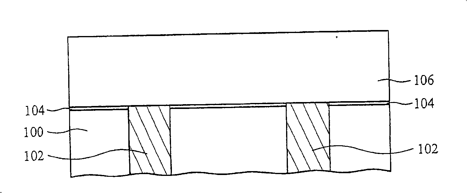
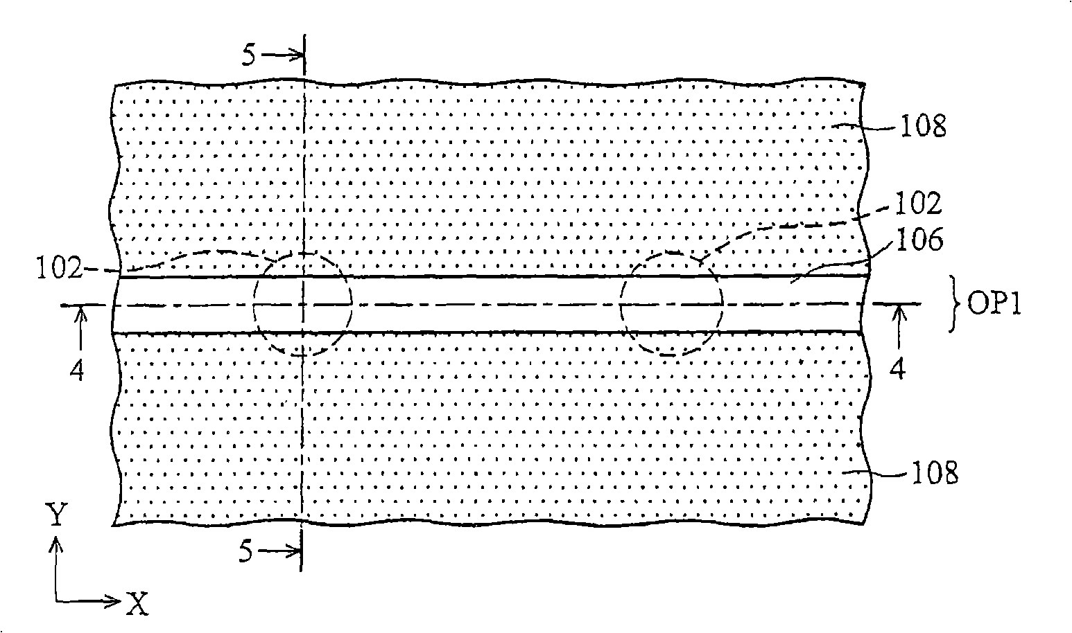
[0046] Embodiments of the capacitor of the present invention and its manufacturing method will cooperate with the following and Figure 1-24 Illustrate with the accompanying drawings, where figure 1 , 3 , 6, 9, 12, 15, 18 and 21 are a series of top view diagrams, and figure 2 , 4 , 5, 7, 8, 10, 11, 13, 14, 16, 17, 19, 20, 22 and 23 are a series of cross-sectional schematic diagrams, respectively showing along figure 1 , 3 , 6, 9, 12, 15, 18 and 21 etc. in the drawings, line segment 2-2, line segment 4-4, line segment 5-5, line segment 7-7, line segment 8-8, line segment 10-10, line segment 11-11 , Line 13-13, Line 14-14, Line 16-16, Line 17-17, Line 19-19, Line 20-20, Line 22-22, and Line 23-23 are explained in different steps The production situation in . and Figure 24 Then it is a three-dimensional schematic diagram showing a capacitor structure according to another embodiment of the present invention.

[0047] Please also refer to figure 1 and figure 2Firstly, ...


PUM


Abstract

The invention discloses a capacitor and a method for preparing the capacitor, wherein the capacitor comprises a dielectric layer, a first conducting layer which is positioned on the dielectric layer, a supporting rib which extends along a first direction and is embedded in the first conducting layer, a second conducting layer which extends along a second direction which is perpendicular to the first direction and is embedded in the first conducting layer, wherein a part of the second conducting layer is transversely arranged on the supporting rib and is supported by the supporting rib, and the dielectric layer is arranged between the second conducting layer and the first conducting layer and electrically separates the second conducting layer and the first conducting layer.

Description

technical field [0001] The present invention relates to a semiconductor memory device, and in particular to a capacitor for the semiconductor memory device and a manufacturing method thereof. Background technique [0002] Dynamic random access memory (DRAM) is a kind of volatile memory, which stores digital signals by charging / discharging capacitors therein. When the power supplied to the above-mentioned DRAM is turned off, the data stored in the memory will be completely erased. Generally, a DRAM includes at least one field effect transistor (FET) and a capacitor, wherein the capacitor is used to store a signal of a storage unit in the DRAM. [0003] In recent years, with the trend of reducing the size of memory cells in DRAM, although the size of memory cells has been gradually reduced, the capacitors in memory cells still have to have a certain storage capacitance value and cannot be gradually reduced with the trend of size reduction. , in order to store the signal. ...

Claims


Application Information

Patent Timeline
IPC IPC(8): H01L27/00H01L27/108H01L21/02H01L21/82H01L21/8242
Inventor 吴孝哲李名言蔡文立
Owner PROMOS TECH INC
Why Eureka
Try Eureka