Capacitor and manufacturing method thereof

A manufacturing method and capacitor technology, applied in semiconductor/solid-state device manufacturing, electric solid-state devices, circuits, etc., can solve the problems of limited manufacturing space size, difficulty in integrating capacitors, high process temperature and process execution time, etc.

Inactive Publication Date: 2009-01-21
PROMOS TECH INC
View PDF0 Cites 0 Cited by
  • Summary
  • Abstract
  • Description
  • Claims
  • Application Information

AI Technical Summary

Problems solved by technology

[0005] However, the above-mentioned application technology of growing hemispherical dies of silicon materials usually requires extremely high process temperature and process execution time, and the size of the grown hemispherical dies is often limited by the size of the capacitor manufacturing space such as trenches. , so it is not easy to integrate in the fabrication of DRAM using capacitors placed in trenches

Method used


Image

  • Capacitor and manufacturing method thereof
  • Capacitor and manufacturing method thereof
  • Capacitor and manufacturing method thereof

Examples


Embodiment Construction

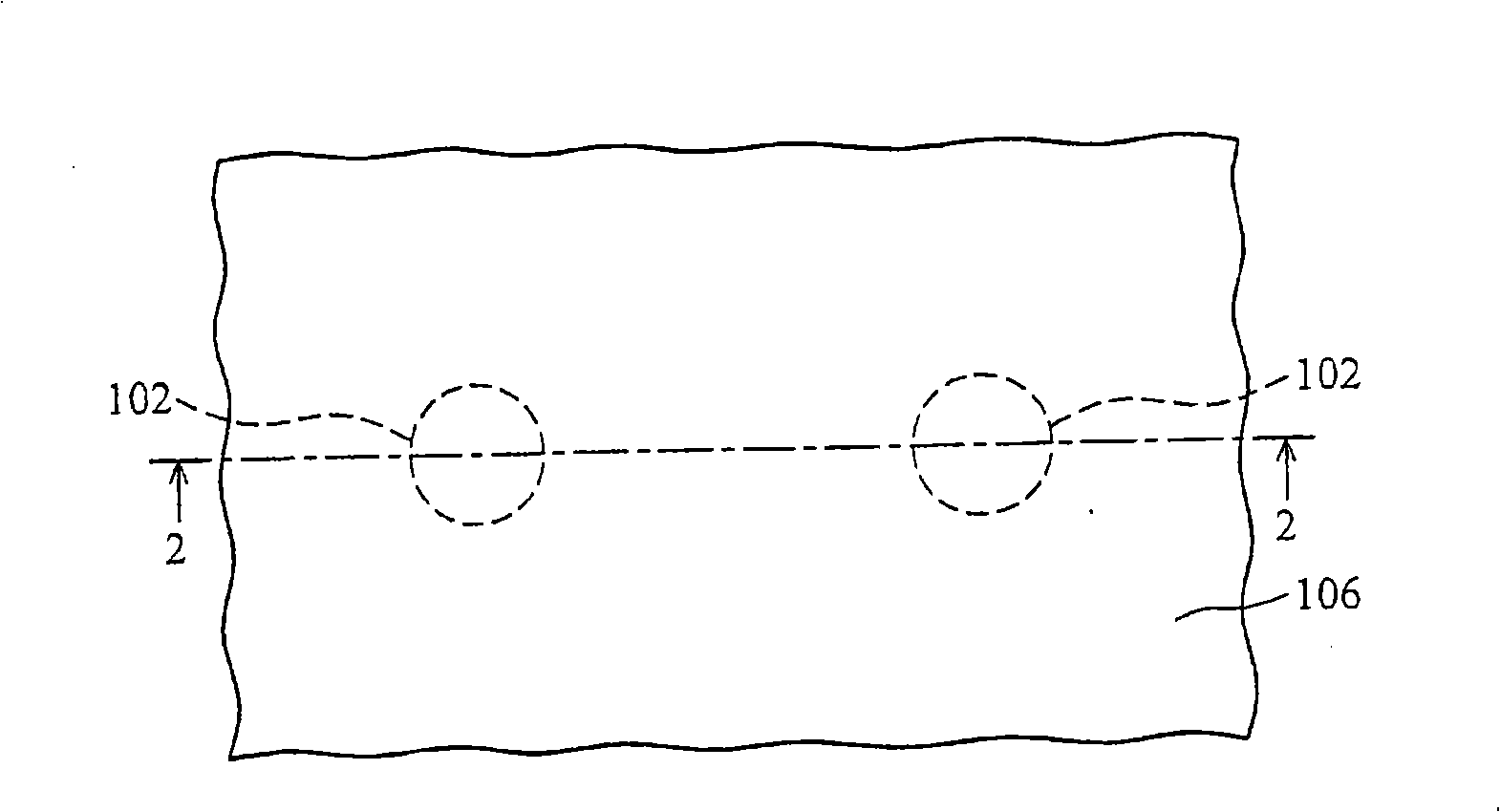
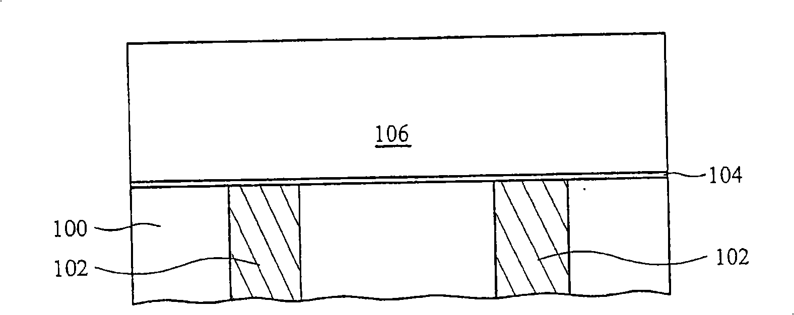
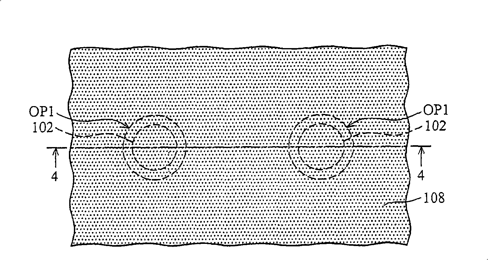
[0029] The embodiment of the capacitor and its manufacturing method of the present invention will cooperate with the following and Figure 1-12 Exemplified by the scheme of figure 1 , 3 , 5, 7, 9 and 11 are a series of top view diagrams, and figure 2 , 4 , 6, 8, 10 and 12 are a series of schematic cross-sectional diagrams, which respectively show the figure 1 , 3 The cross-sections of the line segments 2-2, 4-4, 6-6, 8-8, 10-10, and 12-12 in 5, 7, 9, and 11 are used to explain the production in different steps.

[0030] Please also refer to figure 1 versus figure 2 First, a semiconductor structure is provided. The semiconductor structure includes a pair of conductive contacts 102 disposed in the dielectric layer 100. Here, the semiconductor structure may further include a semiconductor substrate (not shown) and a plurality of transistors (not shown) formed on the semiconductor substrate, and the conductive contacts 102 respectively electrically contact one of the transistors p...


PUM


Abstract

The invention discloses a capacitor and a method for preparing the capacitor, wherein the capacitor comprises a first dielectric layer, a plow groove which is arranged in the first dielectric layer and is provided with a first diameter, a first conducting layer which is adaptively arranged in the plow groove and on the bottom and the side wall of the first dielectric layer which are exposed outside the plow groove, a plurality of conducting inserted pins which are arranged on the bottom of the first conducting layer, the conducting inserted pins are apart with a certain distance with each other, a capacitance layer which is adaptively arranged on the conducting inserted pins and the surface of the first conducting layer, and a fourth conducting layer which covers on the capacitance layer, wherein the second conducting layer, the conducting inserted pins and the first conducting layer are electrically insulated by the capacitance layer. The invention further provides a corresponding method to form the capacitor.

Description

Technical field [0001] The present invention relates to a semiconductor storage device, and more particularly to a capacitor used in the semiconductor storage device and a manufacturing method thereof. Background technique [0002] A dynamic random access memory (DRAM) is a volatile memory, and its storage of digital signals is achieved by charging / discharging a capacitor in it. When the power supply to the above-mentioned dynamic random access memory is turned off, the data stored in the memory will be completely erased. Generally speaking, a dynamic random access memory includes at least a field effect transistor (FET) and a capacitor (capacitor), where the capacitor is used to store the signal of the memory cell in the dynamic random access memory. [0003] In recent years, with the shrinking trend of the memory cell size of dynamic random access memory, although the size of the memory cell is gradually shrinking, the capacitor in the memory cell must still have a certain amou...

Claims


Application Information

Patent Timeline
Patent Type & Authority Applications(China)
IPC IPC(8): H01L27/108H01L23/522H01L21/8242H01L21/768
Inventor 吴孝哲李名言蔡文立
Owner PROMOS TECH INC
Why Eureka
Try Eureka