Phase changeable storage device and manufacture method thereof

A technology of phase change storage and manufacturing method, applied in information storage, static storage, digital storage information, etc., can solve problems such as inability to further provide solutions for increasing current density, limited shrinkage, and limited heating electrodes 16

Active Publication Date: 2010-01-27
POWERCHIP SEMICON MFG CORP
View PDF3 Cites 0 Cited by
  • Summary
  • Abstract
  • Description
  • Claims
  • Application Information

AI Technical Summary

Problems solved by technology

[0007] However, the diameter D0 of the heating electrode 16 is still limited by the capability of the current photolithography process, and thus its shrinkage is limited, so it cannot further provide a solution for increasing the current density, which is not conducive to the development of the phase change memory cell structure. miniature

Method used


Image

  • Phase changeable storage device and manufacture method thereof
  • Phase changeable storage device and manufacture method thereof
  • Phase changeable storage device and manufacture method thereof

Examples


no. 1 example

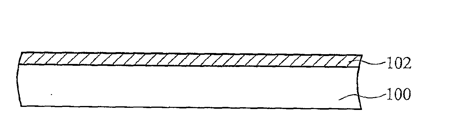
[0058] Please refer to figure 2 Firstly, a substrate 100 is provided, such as a substrate of semiconductor material such as a silicon substrate, on which elements and film layers such as transistors or diodes and dielectric layers can be disposed. In order to simplify the illustration, the substrate 100 is only shown as a flat substrate without showing the film layers and elements formed thereon.

[0059] Please refer to image 3 , and then form a layer of conductive material on the substrate 100 and pattern it through subsequent photolithography and etching processes (not shown), thereby forming the conductive layer 102 on the substrate 100 . The material of the conductive layer 102 can be polysilicon, aluminum, tungsten and other conductive materials. The conductive layer 102 is used as a bottom electrode.

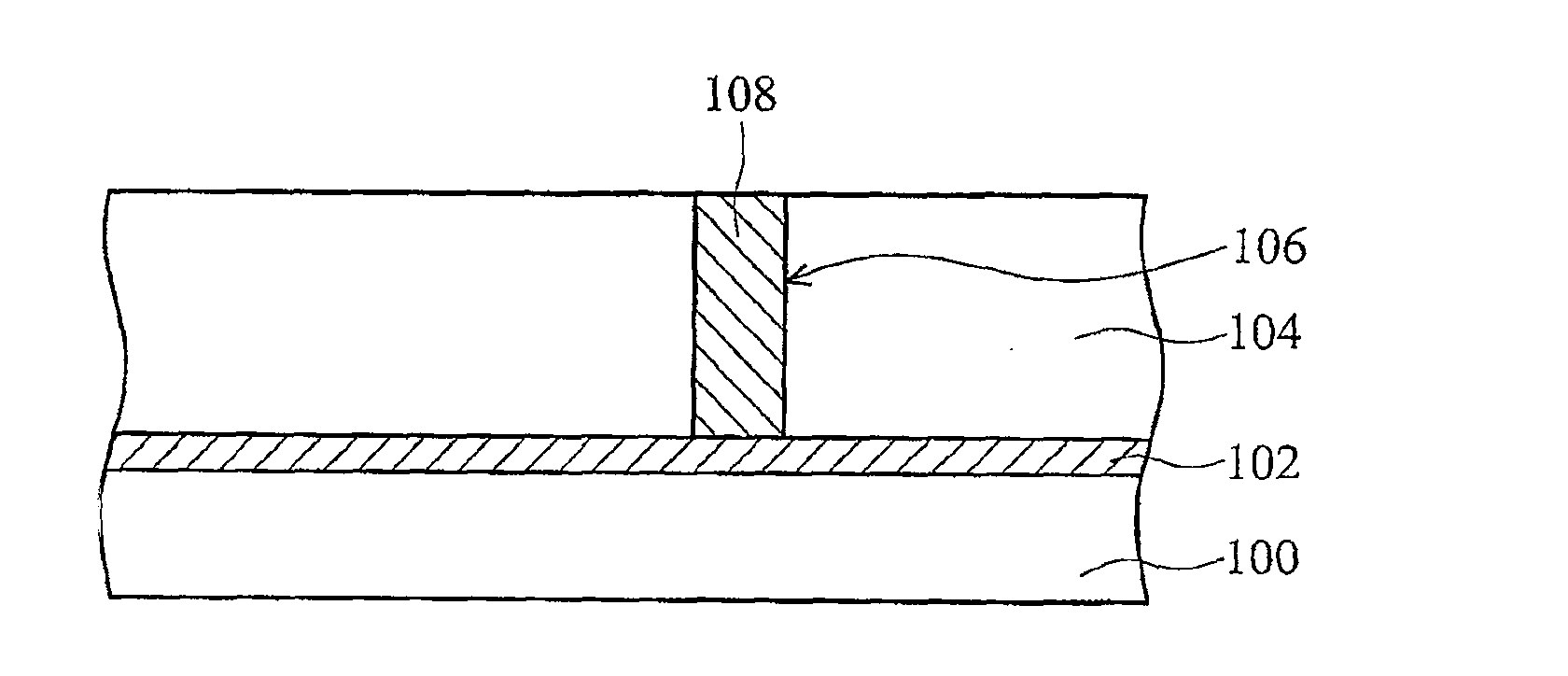
[0060] Please refer to image 3, and then form a dielectric layer 104 on the conductive layer 102, the material of the dielectric layer 104 is, for example, boropho...

no. 2 example

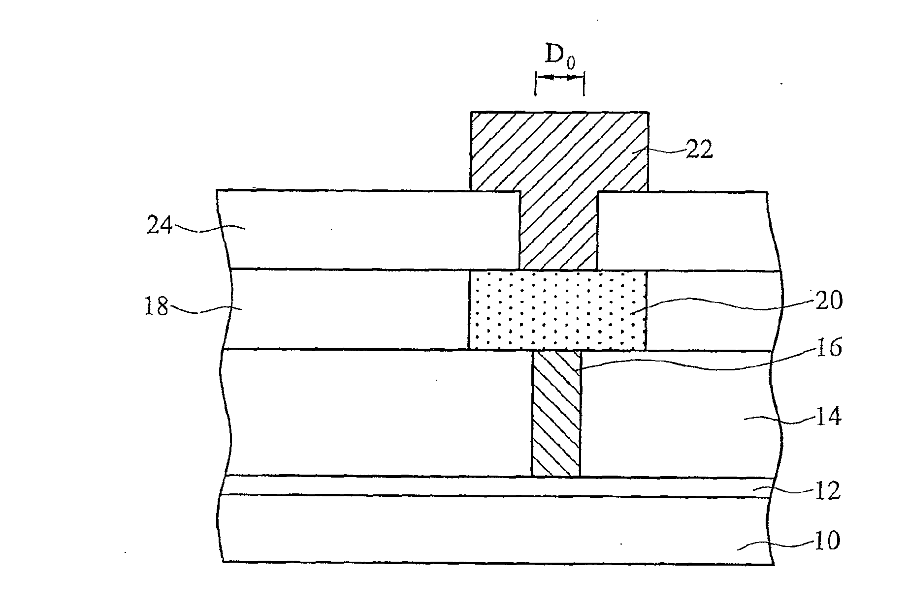
[0070] Figures 9 to 12 It is a series of schematic diagrams showing the manufacturing method of the phase change memory device according to the second embodiment of the present invention. This embodiment is a modification of the first embodiment, in which some process steps are the same as those of the first embodiment, and only different steps are shown here to simplify the illustration, and the components that are the same as those in the first embodiment are also marked for the same label.

[0071] Please refer to Figure 9 , by as in the first embodiment Figure 2-5 implementation of the described process to provide as Figure 5 The structures shown serve as starting structures. A dielectric layer 140 is then formed overlying the starting structure to planarize the overall surface. Such as Figure 9 shown. A dielectric layer 140 is formed on the dielectric layer 104b and covers the oxide layer 114, and the conductive electrode 108 now includes a reduced portion 108...


PUM

PropertyMeasurementUnit
diameteraaaaaaaaaa

Abstract

Disclosed is a method for reducing the contact area between a heating electrode and a phase-change material layer, including the following steps: a first dielectric layer is provided, inside which a heating electrode is arranged; the heating electrode, at a first diameter, has an exposed part which extends out of the surface of the first dielectric layer; oxidation process is carried out so as to develop an oxide layer on the top of the exposed part and the side wall of the heating electrode, then the diameter of the exposed part is reduced to a second diameter which is smaller than the first diameter; part of the oxide layer is removed so as to expose the top of the exposed part of the heating electrode, and oxide spacer material is left on the side wall of the exposed part of the heating electrode; a phase-change material layer is formed on the exposed part of the heating electrode, making sure that the phase-change material layer at least contacts with the top of the exposed part and the top of the oxide spacer material.

Description

technical field [0001] The present invention relates to a memory device, in particular to a phase-change memory device and a manufacturing method thereof. Background technique [0002] Phase-change memory has the characteristics of non-volatility, high read signal, high density, high erasure and write times, and low operating voltage / current, and it is a non-volatile memory with great potential. Among them, improving storage density and reducing operating current are important technical indicators. [0003] Phase-change materials can exhibit at least two solid states, including crystalline and amorphous states. Generally, changes in temperature are used to switch between the two states. Due to the disordered arrangement of atoms in the amorphous state, it has high resistance. Therefore, through simple The crystalline state and the amorphous state of the phase change material can be easily distinguished by electrical measurement. Since the phase transition of phase change m...

Claims


Application Information

Patent Timeline
Patent Type & Authority Patents(China)
IPC IPC(8): H01L45/00H01L27/24G11C11/56
Inventor 林永发王德纯
Owner POWERCHIP SEMICON MFG CORP
Why Eureka
Try Eureka