

Electrooptical device, electronic apparatus, and method for producing electrooptical device
An electro-optical device and manufacturing method technology, applied in semiconductor/solid-state device manufacturing, circuits, electrical components, etc., can solve problems such as differences in ink thickness, differences, and inability to achieve light emission
- Summary
- Abstract
- Description
- Claims
- Application Information
AI Technical Summary
Problems solved by technology
Method used
Image

Examples
no. 1 Embodiment approach
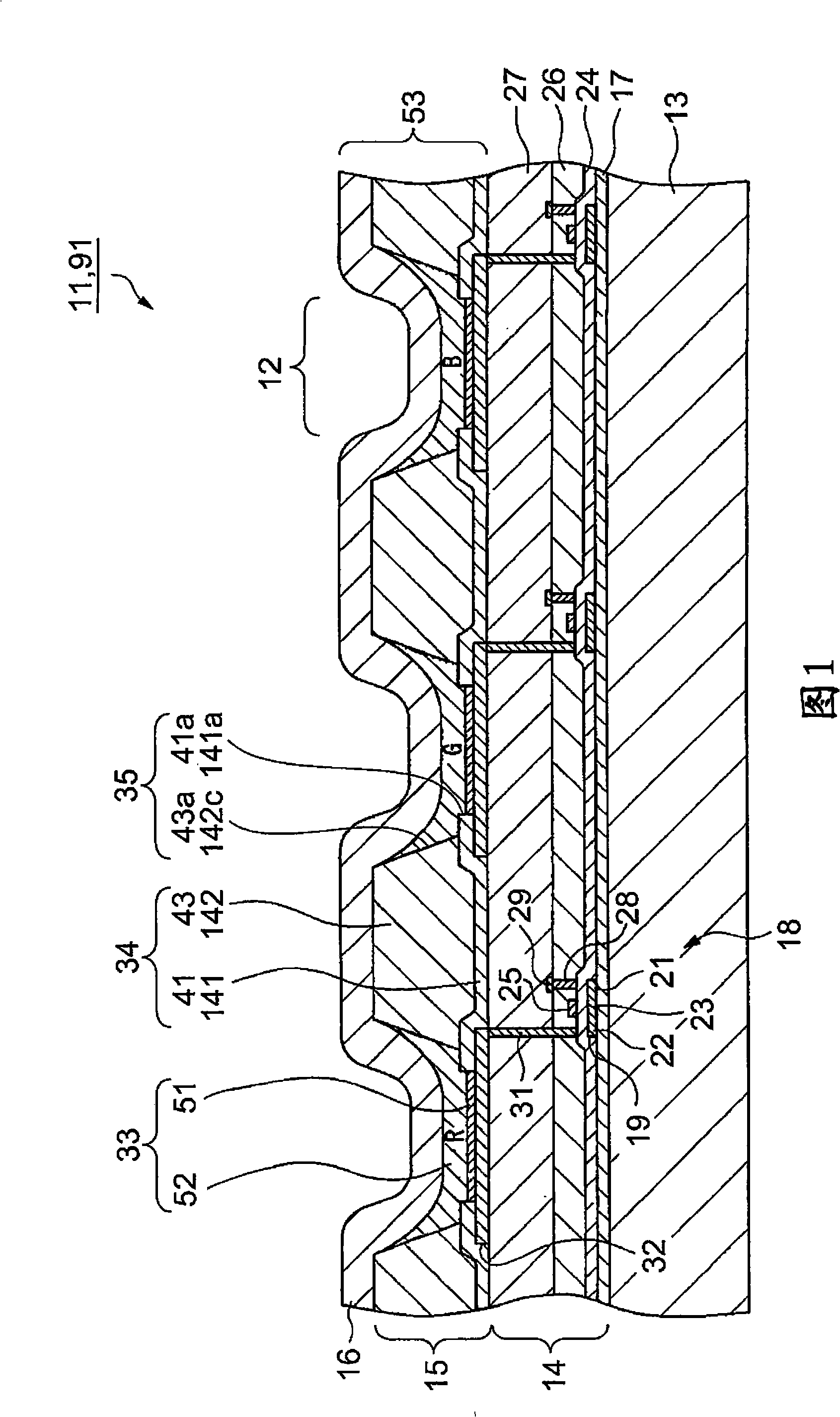
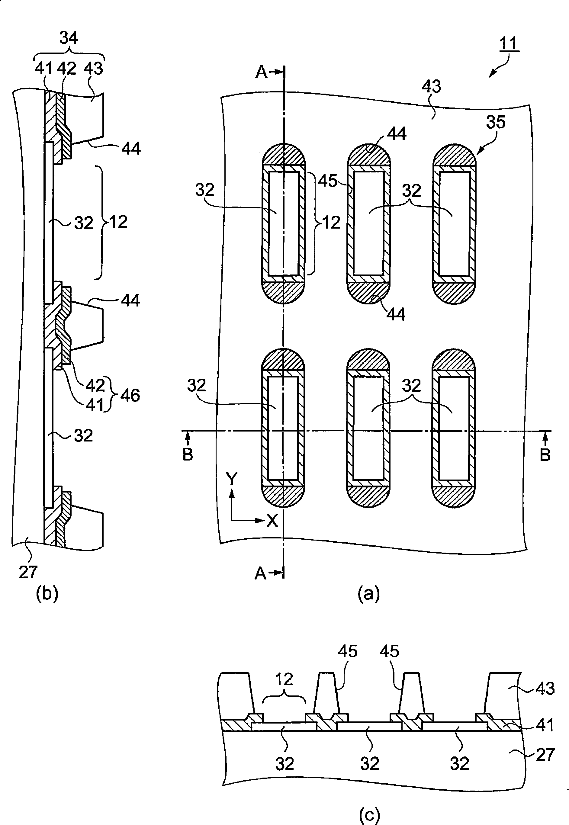
[0090] 1 is a schematic cross-sectional view showing a partial structure of an organic EL device as an electro-optical device according to a first embodiment. figure 2 It is a schematic diagram showing the structure of the cell bank at the stage where the cell bank is formed in the organic EL device. (a) is a schematic plan view of the organic EL device viewed from above, (b) is a schematic cross-sectional view along the A-A section of the organic EL device shown in (a), and (c) is a schematic cross-sectional view along the organic EL device shown in (a). A schematic cross-sectional view of the B-B cross-section of the EL device. In addition, FIG. 1 is a figure which shows the cross-sectional positional relationship of each component, and the relative positional relationship is not mentioned for now. Referring to Figure 1 below, figure 2 The structure of the organic EL device will be described.
[0091] As shown in FIG. 1, an organic EL device 11 emits light in a light emit...
no. 2 Embodiment approach
[0137] Figure 5 It is a schematic diagram which shows the structure of the storage cell cofferdam of 2nd Embodiment. (a) is a schematic plan view of the organic EL device viewed from above, (b) is a schematic cross-sectional view along the A-A section of the organic EL device shown in (a), and (c) is a schematic cross-sectional view along the organic EL device shown in (a). A schematic cross-sectional view of the B-B cross-section of the EL device. Below, refer to Figure 5 , to illustrate the structure of the storage cell cofferdam. In addition, the structure of the storage cell cofferdam in the second embodiment differs from that in the first embodiment in that the first lower storage cell cofferdam is formed on the lower side of the upper storage cell cofferdam in the area on the arc side. The lower storage cell cofferdam is not formed in the area of the straight line. Hereinafter, the same reference numerals are assigned to the same components as those in the first ...
no. 3 Embodiment approach
[0143] Figure 6 It is a schematic diagram which shows the structure of the storage cell cofferdam of 3rd Embodiment. (a) is a model top view of the storage cell cofferdam viewed from above, (b) is a model section view along the A-A section of the storage cell cofferdam shown in (a), (c) is a model view along the cell cofferdam shown in (a) The model section diagram of the B-B section of the storage cell cofferdam. Below, refer to Figure 6 , to illustrate the structure of the storage cell cofferdam. In addition, the structure of the cell cofferdam of the third embodiment differs from that of the first embodiment in that only the second lower cell cofferdam is formed on the lower side of the upper layer cell cofferdam in the region of the straight line portion. Hereinafter, the same reference numerals are assigned to the same components as those in the first embodiment, and descriptions thereof will be omitted or simplified.
[0144] Such as Figure 6 As shown, in the are...
PUM
 Abstract
Description
Claims
Application Information