Large scale atomic gate nanometer measuring device
A measuring device and atomic grid technology, applied in measuring devices, electromagnetic measuring devices, electrical devices, etc., can solve the problem of not being able to engrave integrated circuit chip patterns, and achieve the effect of increasing the measuring range
- Summary
- Abstract
- Description
- Claims
- Application Information
AI Technical Summary
Problems solved by technology
Method used
Image

Examples
Embodiment Construction
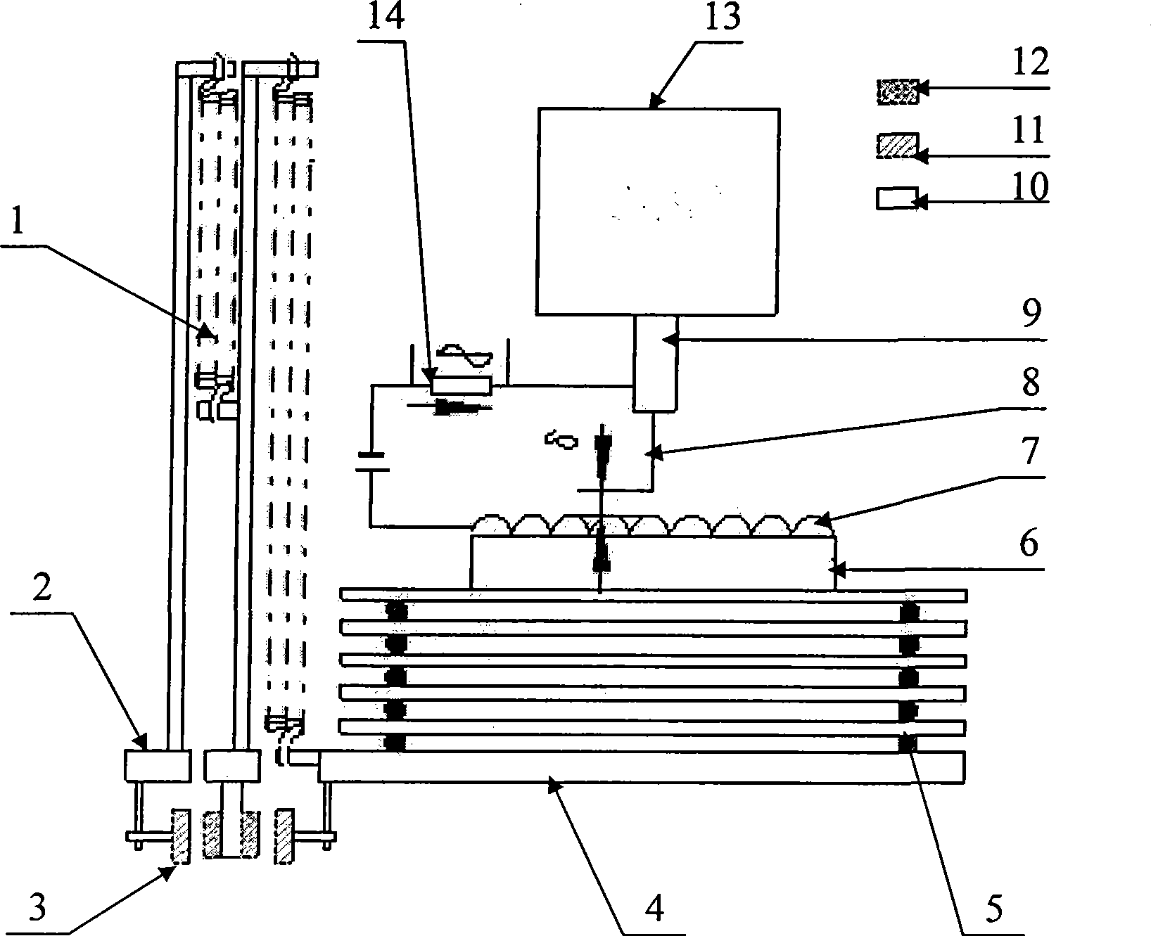
[0017] Such as figure 1 Middle, 1—vibration damping spring, 2—bracket, 3—magnetic vibration damping system, 4—base, 5—combined vibration damping platform, 6—nanometer feed table, 7—atom grid, 8—probe, 9 — Piezoelectric ceramic driver, 10 — stainless steel block, 11 — copper block, 12 — magnet, 13 — scanning tunneling microscope, 14 — signal collector.
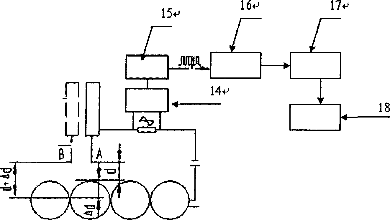
[0018] figure 2 Among them, 14—signal collector, 15—pulse circuit, 16—counter, 17—computer, 18—display printing equipment.
[0019] The large-scale atomic grid nano-measurement device of the present invention includes a multi-stage damping system, which consists of two damping springs 1 arranged on the bracket 2 to form a two-stage spring damping, and then through the magnetic damping system 3 and a combined damping platform 5, wherein the magnetic damping system 3 includes stainless steel block 10, copper block 11, magnet 12 and other components, the damping spring 1 and the magnetic damping system 3 are connected with the ...
PUM
 Abstract
Description
Claims
Application Information