Multiband antenna using photonic band gap material

A technology of photonic bandgap materials and multi-band antennas, which is applied to antennas, antenna parts, waveguide devices, etc., can solve the problems of large basic size and limit the application of PBG, and achieve the effect of simple structure and reduced manufacturing cost

Inactive Publication Date: 2013-01-16
PANASONIC CORP
View PDF0 Cites 0 Cited by
  • Summary
  • Abstract
  • Description
  • Claims
  • Application Information

AI Technical Summary

Problems solved by technology

However, for the microwave band gap with a working frequency of GHz, if the usual all-dielectric material is used, such a design requirement will make the basic size of the material too large, which greatly limits the application of PBG in the field of microwave communication.

Method used


Image

  • Multiband antenna using photonic band gap material
  • Multiband antenna using photonic band gap material
  • Multiband antenna using photonic band gap material

Examples


no. 1 example

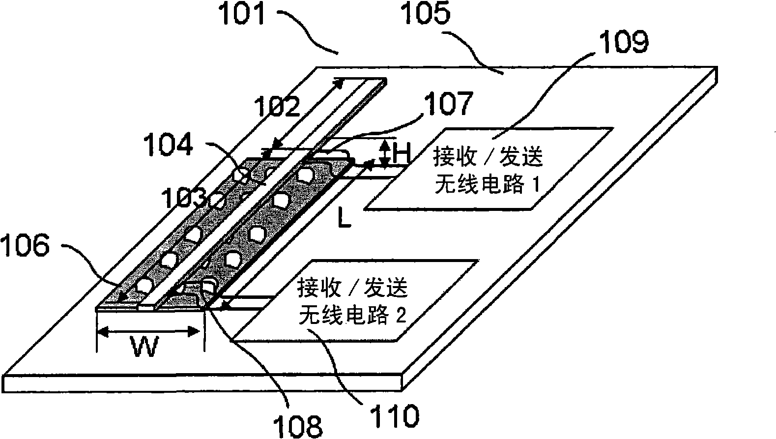
[0022] Refer below figure 2 A first embodiment of the structure of a multiband antenna using a photonic bandgap material is described. Such as figure 2 As shown, the antenna device according to this embodiment includes a microstrip antenna 104, a substrate 105, a photonic bandgap material plate 106, a first feed line 107, a second feed line 108, a first receiving / transmitting wireless circuit 109, a second electric circuit Receive / transmit wireless circuit 110.

[0023] In the antenna device 101 of this embodiment, the photonic bandgap material plate 106 is disposed on the substrate 105 and is in close contact with the substrate 105 . The microstrip antenna 104 is disposed on the photonic bandgap material plate 106 along the length direction of the photonic bandgap material plate 106 , that is, the length direction of the microstrip antenna 104 is the same as that of the photonic bandgap material plate 106 . The length of the microstrip antenna 104 is longer than the leng...

no. 2 example

[0036] In the first embodiment, the PBG material is used to be in close contact with the second antenna unit 103 to realize reception / transmission of multi-band signals.

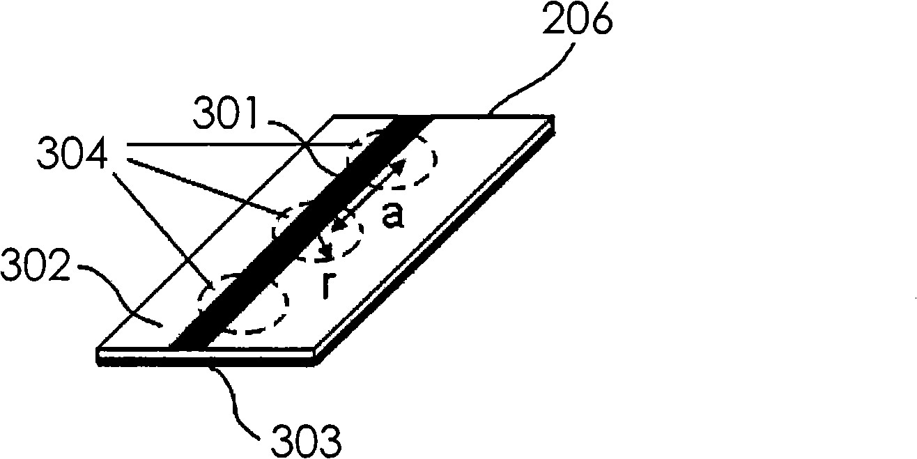
[0037] Since the use of PBG materials will increase the cost of the antenna, sometimes PBG materials cannot be used to realize the multi-band antenna due to cost considerations. A second embodiment of the present invention provides a multi-band antenna device obtained by processing a printed circuit board to realize a PBG configuration. The cost of the multi-band antenna device according to the second embodiment is very low, even negligible.

[0038] In the prior art, it is proposed to process a periodic structure on a printed circuit board to realize a PBG structure. image 3 A schematic structural diagram of a PBG structure according to the second embodiment of the present invention is shown. Such as image 3 As shown, the PBG structure used in the second embodiment includes a microstrip antenna 204 , a...


PUM


Abstract

A multiband antenna device made of a photonic band gap material comprises a micro-strip antenna, a first antenna unit taken as one part of the microstrip antenna and used for receiving / transmitting the signal of the first bandwidth, and a second antenna unit taken as one part of the microstrip antenna; the second antenna unit is in tight contact with a photonic band gap material board made of the photonic band gap material, and is integrated with the first antenna unit and used for receiving / transmitting the signal of the second bandwidth; wherein, the photonic band gap material board made of the photonic band gap material has band stop property towards the first bandwidth. Additionally, the photonic band gap material board made of the photonic band gap material can be replaced by a photonic band gap structure board made from a printed circuit board.

Description

technical field [0001] The present invention relates to a multi-band antenna using a photonic bandgap material, in particular to utilizing the band-stop characteristic of a photonic bandgap (PBG) material to realize multi-band transmission / reception of the antenna without increasing the size of the antenna. Background technique [0002] As wireless receiving devices increase in mobile terminals, the number of receiving / transmitting antennas also increases simultaneously. On the other hand, with the improvement of the integration of electronic equipment, the volume of communication equipment is getting smaller and smaller, which requires the antenna to reduce its own size. Reducing the size of an antenna without compromising its gain and efficiency is a daunting task. The improvement of the integration of electronic equipment often requires an antenna to support two or more wireless services in a wide frequency range, and broadband and multi-band antennas can meet such needs...

Claims


Application Information

Patent Timeline
Patent Type & Authority Patents(China)
IPC IPC(8): H01Q1/00H01Q13/08H01P1/20
CPCH01P1/2005
Inventor 李楠刘健
Owner PANASONIC CORP
Why Eureka
Try Eureka