Light emitting device

一种发光装置、发光元件的技术,应用在半导体器件、电气元件、电路等方向,能够解决不公知调整等问题,达到防止自吸收、提高光提取效率的效果

Inactive Publication Date: 2009-03-04
RESONAC HOLDINGS CORPORATION
View PDF3 Cites 0 Cited by
  • Summary
  • Abstract
  • Description
  • Claims
  • Application Information

AI Technical Summary

Problems solved by technology

However, it is not known to adjust the geometry of a light-emitting device mounted with a light-emitting element to improve light extraction efficiency.

Method used


Image

  • Light emitting device
  • Light emitting device
  • Light emitting device

Examples


example 1

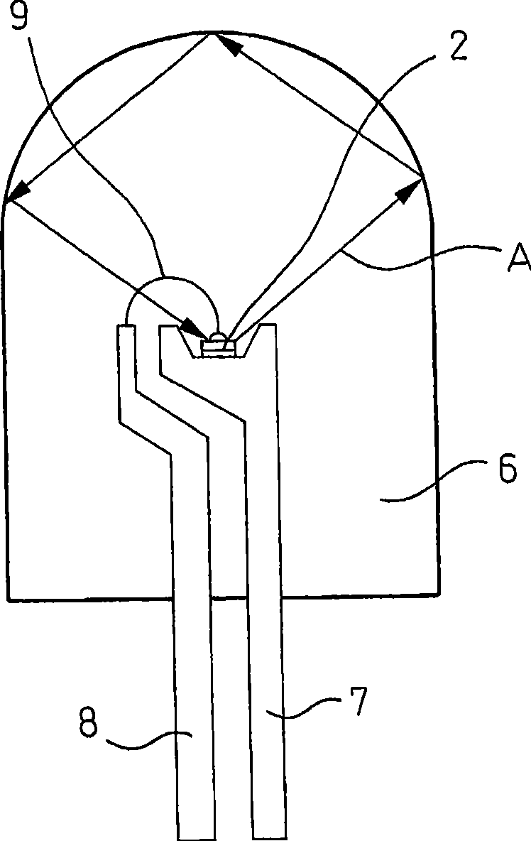
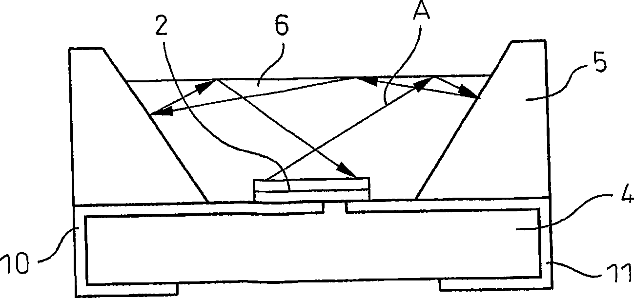
[0078] A first example of a light emitting device according to the present invention will now be described with reference to the accompanying drawings. Figure 14 is a cross-sectional view of the light-emitting device fabricated in this example, Figure 15 is a plan view of the light emitting device. The light emitting device 111 is composed of a heat sink 104 , a reflector 105 , a carrier 103 , a semiconductor light emitting element 102 and a cap 101 . Reference numeral 106 represents a sealing compound. In addition, reference numeral 120 denotes an external power supply connection electrode, and 121 denotes a heat sink mounting portion.

[0079] The used semiconductor light emitting element 102 described below is a GaN-based compound semiconductor blue light emitting element having a square shape with sides of 1 mm×1 mm and a thickness of about 90 μ.

[0080] A base layer composed of undoped GaN with a thickness of 8 μm, a Ge-doped n-type GaN contact layer with a thicknes...

example 2

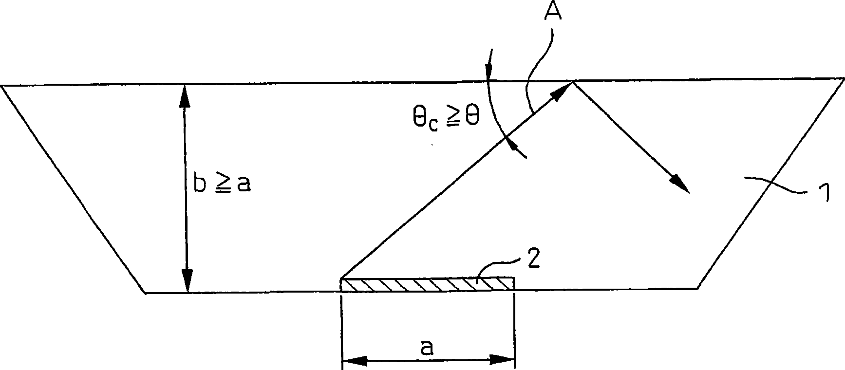
[0099] Figure 17A cross-sectional view of a light-emitting device fabricated in this example is shown. Except that the shape of the cap is a truncated conical shape, a light-emitting device was manufactured in the same manner as in Example 1, the truncated conical shape has a top surface radius of 0.8 mm, a bottom surface radius of 1.6 mm, and a height of 1.5 mm, The area ratio of the top surface to the bottom surface is 1:4 and the interval between the top surface and the bottom surface is larger than the longest diagonal of the light emitting element. When the obtained light-emitting device was subjected to a current test in the same manner as in Example 1, the light extraction was about 1.87 times that of the bare chip.

[0100] When comparing the front luminance of the light emitting device of Example 1 and the light emitting device of Example 2, the luminance of the light emitting device of Example 1 was 1, and the luminance of the light emitting device of Example 2 was...


PUM


Abstract

An object of the present invention is to provide a light emitting device with excellent light extraction efficiency due to reduced self-absorption of light from the light emitting element. The inventive light emitting device comprises a board, a semiconductor light emitting element formed on the board optionally via a submount, a cap sealing the semiconductor light emitting element and a reflector provided surrounding the cap, wherein the cap has top and bottom surfaces that are parallel to the top surface of the semiconductor light emitting element, and the spacing between the top and bottom surfaces is 1-3 times the longest diagonal or the diameter of the semiconductor light emitting element.

Description

[0001] Cross References to Related Applications [0002] This application is based upon an application filed under 35 U.S.C. §111(a) pursuant to 35 U.S.C. §119(e)(1), claiming Provisional Application No. 60 filed February 23, 2006 under 35 U.S.C. §111(b) The preferred right of / 775,798. technical field [0003] The present invention relates to light emitting devices, and in particular, to light emitting devices with improved light extraction efficiency. Efficiency is improved by reducing self-absorption of light from the light emitting element due to total reflection of light at a light extraction surface formed of a lens or sealing material covering the light emitting element. Background technique [0004] Examples of known light-emitting devices using light-emitting elements include, for example, figure 1 A light-emitting device shown in , which has a resin-sealed lamp-type light-emitting diode mounted on a lead frame, and has, for example, figure 2 A light-emitting de...

Claims


Application Information

Patent Timeline
Patent Type & Authority Applications(China)
IPC IPC(8): H01L33/00H01L33/06H01L33/32H01L33/54H01L33/60H01L33/62
CPCH01L33/54H01L33/60H01L2224/48091H01L2224/48247H01L2224/73265H01L2924/181H01L2924/00012H01L2924/00014
Inventor 保科孝治
Owner RESONAC HOLDINGS CORPORATION
Why Eureka
Try Eureka