Shifting register and LCD
A shift register, shift register unit technology, applied in the direction of static memory, static indicator, digital memory information, etc., can solve the problem of overlapping output signals of the shift register, and achieve the effect of avoiding chromatic aberration
- Summary
- Abstract
- Description
- Claims
- Application Information
AI Technical Summary
Problems solved by technology
Method used
Image
Examples
Embodiment Construction
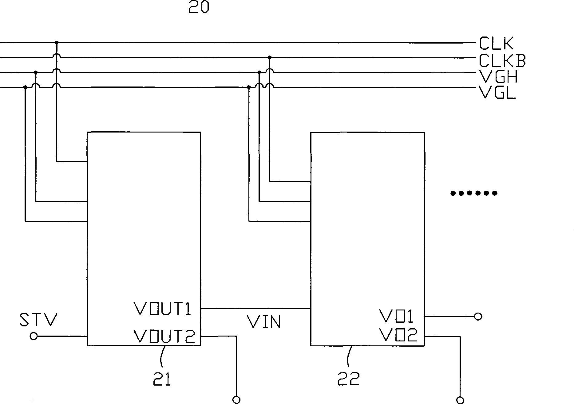
[0025] see image 3 , is a structural frame diagram of a preferred embodiment of the shift register of the present invention. The shift register 20 includes a plurality of shift register units with the same circuit structure, and the plurality of shift register units are connected in series sequentially to receive the first clock signal CLK provided by the external circuit and the clock signal inverted to the first clock signal CLK in sequence. The second clock signal CLKB, the high level signal VGH and the low level signal VGL. Each shift register unit is composed of a plurality of NMOS transistors, and each NMOS transistor includes a gate, a source and a drain. Now take the first shift register unit 21 and its adjacent second shift register unit 22 as an example to illustrate the connection relationship of the shift register 20. The first shift register unit 21 includes an input signal terminal S TV, a A first output terminal VOUT1 and a second output terminal VOUT2. The ...
PUM
 Abstract
Description
Claims
Application Information


