Multiple gate field effect transistor structure and method for fabricating same

A field-effect transistor, multi-gate technology, used in transistors, semiconductor/solid-state device manufacturing, semiconductor devices, etc.

Inactive Publication Date: 2009-03-18
SOITEC SA
View PDF0 Cites 13 Cited by
  • Summary
  • Abstract
  • Description
  • Claims
  • Application Information

AI Technical Summary

Problems solved by technology

However, this results in recessed or undercut fins

Method used


Image

  • Multiple gate field effect transistor structure and method for fabricating same
  • Multiple gate field effect transistor structure and method for fabricating same
  • Multiple gate field effect transistor structure and method for fabricating same

Examples


Embodiment Construction

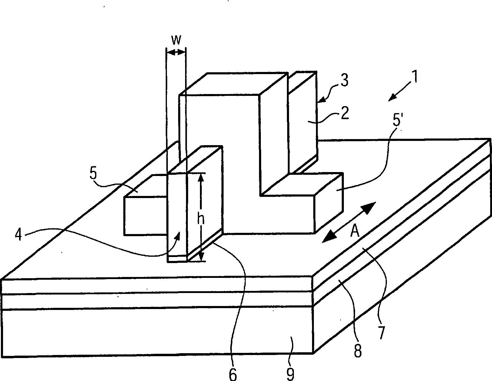
[0024] figure 1Taking FinFET structure 1 as an example schematically and in principle shows the main part of the MuGFET structure. The FinFET 1 comprises a fin structure 2 formed from an active semiconductor top layer of an SOI type substrate. In the example shown, the semiconductor top layer (and thus the fin 2 ) consists of silicon, wherein in other not shown embodiments of the invention, the fin 2 can be made of, for example, strained silicon, SiGe, SiC, Ge and / or A (III)-B(V) compounds such as other semiconductor materials.

[0025] As an improvement, strained silicon can be used instead of the top silicon layer of the SOI type substrate. Using a strained silicon layer greatly improves electron mobility in the (100) orientation of silicon, thereby providing higher transistor currents.

[0026] exist figure 1 In , the height h of the fin 2 is about 50 nm, but in other not shown embodiments of the present invention may be between 30 nm and 100 nm. The width w of the fin...


PUM


Abstract

The present invention relates to a multiple gate field effect transistor structure with a fin-like structure for forming therein a transistor channel of the Multiple Gate Field Effect Transistor structure, the fin-like structure being formed from at least one active semiconductor layer of a SOI type structure on a buried insulator of said SOI type structure, and a method for fabricating same, said method comprising providing a SOI type substrate comprising at least one active semiconductor layer, a buried insulator and a carrier substrate, and forming from said semiconductor layer a fin-like structure on the insulator, the fin-like structure forming a region for a transistor channel of the Multiple Gate Field Effect Transistor structure. It is the object of the present invention to provide a multiple gate field effect transistor structure and a method for fabricating same, wherein the multiple gate field effect transistor structure can be near ideally prepared to overcome several related issues.

Description

technical field [0001] The present invention relates to a multi-gate field effect transistor structure having a fin structure in which a transistor channel of the multi-gate field effect transistor structure is formed, and a method for manufacturing the same. - On-Insulator) (silicon-on-insulator) type structure on a buried insulator formed from at least one active semiconductor layer of said SOI type structure, said method comprising the steps of: providing a SOI type substrate comprising at least one active semiconductor layer, a buried insulator, and a carrier substrate; and forming a fin structure on said insulator from said semiconductor layer, said fin structure forming a multi-gate field effect transistor structure The region of the transistor channel. Background technique [0002] Device scaling is a major factor driving improvements in integrated circuit fabrication. Scaling conventional planar MOSFET devices beyond the 32nm process is difficult, if not impossible...

Claims


Application Information

Patent Timeline
Patent Type & Authority Applications(China)
IPC IPC(8): H01L21/336H01L29/78H01L29/786
CPCH01L29/78603H01L29/7853H01L29/785H01L29/66795H01L29/42392H01L29/78696H01L29/772
Inventor 保罗·帕特诺
Owner SOITEC SA
Why Eureka
Try Eureka