Copper surface treatment liquid and copper surface treatment method for multilayer printed circuit board manufacturing

A technology of printed circuit boards and processing methods, which is applied in the direction of metal material coating technology, etc., can solve the problems of difficult to balance lamination bonding force and signal loss, and achieve the effect of copper surface roughening, anti-corrosion, and strong affinity

Active Publication Date: 2019-07-19
UNIV OF ELECTRONIC SCI & TECH OF CHINA +1
View PDF13 Cites 5 Cited by
  • Summary
  • Abstract
  • Description
  • Claims
  • Application Information

AI Technical Summary

Problems solved by technology

[0005] In view of the above, aiming at the problem that the existing copper surface treatment for multilayer printed circuit board manufacturing is difficult to take into account the lamination bonding force and signal loss, the present invention provides a copper surface treatment liquid for multilayer printed circuit board manufacturing and The treatment method is to divide the copper surface roughening and the pe

Method used


Image

  • Copper surface treatment liquid and copper surface treatment method for multilayer printed circuit board manufacturing
  • Copper surface treatment liquid and copper surface treatment method for multilayer printed circuit board manufacturing
  • Copper surface treatment liquid and copper surface treatment method for multilayer printed circuit board manufacturing

Examples


Embodiment 1

[0050] (1) Preparation of materials and treatment liquid;

[0051] Take a piece of single-sided copper foil for printed circuit board manufacturing with a copper layer thickness of 18μm, and cut it into a 40mm×80mm sample board with a cutter;

[0052] Preparation of acidic cleaning solution: Weigh 50mL of 98% concentrated sulfuric acid, add it to 800ml of deionized water under constant stirring, then add ionized water to the 1L mark, stir evenly and then leave to cool;

[0053] Alkaline washing solution preparation: Weigh 50g sodium carbonate, 15g sodium bicarbonate, 20g sodium octadecylbenzene sulfonate, and dissolve them in 1000ml deionized water;

[0054] Preparation of the first treatment solution: respectively measure 30g sodium peroxide, 40g sodium hydroxide, 40g sodium silicate, 50g ethylenediaminetetraacetic acid disodium salt, 4g benzotriazole, 5.4g polyethylene glycol, 16g Ammonium molybdate, the order of adding each component under constant stirring is: sodium peroxide→cool...

Embodiment 2

[0084] (1) Inner layer pretreatment;

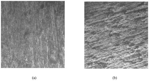
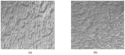
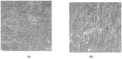
[0085] Take a multi-layer high-frequency high-speed printed circuit board inner layer (line width / line spacing 75μm / 75μm, copper foil thickness 18μm, copper clad substrate (Dk=4.04 / Df=0.0157 at 1GHz) → put it in 32℃ Stir and clean in sulfuric acid pickling solution (5%) for 60 seconds → clean with deionized water → put it into 55℃ sodium carbonate (50g / L) + sodium bicarbonate (15g / L) + dodecyl Wash with sodium sulfonate (20g / L) mixed lotion for 60 seconds → take out and clean with deionized water → dry with hot air;

[0086] (2) Copper surface treatment such as inner layer board circuit;

[0087] Put the cleaned inner layer board into the first copper foil treatment liquid heated to 55℃ and 65℃ respectively, take it out after 120 seconds of treatment, clean it with deionized water, and then treat the first treatment liquid The inner layer board is put into the second copper foil treatment solution, continuously stirred for 120 seconds and then...


PUM


Abstract

The invention relates to copper surface treatment liquid and a copper surface treatment method for multilayer printed circuit board manufacturing, and belongs to the technical field of printed circuits. According to the copper surface treatment liquid and the copper surface treatment method, copper surface roughening and medium layer performance optimization for improving interlayer bonding forceare carried out in two stages, wherein the treatment liquid used for the copper surface roughening comprises alkali metal peroxide, alkali metal hydroxide, alkali metal silicate, polyhydroxylated polymer, a metal complexing agent, a copper metal corrosion inhibitor and a molybdate additive with mass concentrations being 20-50g/L, 30-60g/L, 30-60g/L, 3.5-10g/L, 30-60g/L, 3-8g/L and 6-30g/L respectively; and the treatment liquid used for the medium layer optimization comprises alkali metal sulfide, alkali metal phosphate and a silane coupling agent with the mass concentrations being 10-30g/L, 40-160g/L and 7.5-30g/L respectively. The copper surface treatment liquid has better compatibility with the prior art, the low roughness modification of the copper surface can reach the IPC standard, and the copper surface treatment liquid and the copper surface treatment method are favorable for a multilayer board manufacturing technology to meet the challenge brought by the high frequency of transmission signals of a printed circuit board.

Description

Technical field [0001] The invention belongs to the technical field of printed circuits, and specifically relates to a copper surface treatment liquid for manufacturing a multilayer printed circuit board and a treatment method. Background technique [0002] The concept of 5G (Fifth Generation Communication Technology) has been receiving attention since it was proposed in August 2012. The signal frequency required by 5G is very high, the highest frequency can reach 300GHz, while 4GLTE is 2.6GHz. With the development of electronic technology and the emergence of emerging application fields such as 5G communication technology, Internet of Things, and Internet of Vehicles, high-frequency and high-speed signal high-quality transmission has become a must-have feature of the new generation of printed circuit boards, and communication PCBs are moving towards low roughness. The development of high-density, high-density interconnection and high signal integrity (the quality of the signal ...

Claims


Application Information

Patent Timeline
IPC IPC(8): C23C22/08C23C22/40C23G1/10C23G1/20
CPCC23C22/08C23C22/40C23G1/103C23G1/20
Inventor 王守绪狄梦停何为李清华陈苑明周国云胡志强艾克华
Owner UNIV OF ELECTRONIC SCI & TECH OF CHINA
Why Eureka
Try Eureka