Charge balancing method in current input adc

A technology of charge balance and current, applied in amplifiers with semiconductor devices/discharge tubes, electrical components, physical parameter compensation/prevention, etc., can solve problems such as input current offset errors

Active Publication Date: 2009-03-25
NAT SEMICON CORP
View PDF1 Cites 6 Cited by
  • Summary
  • Abstract
  • Description
  • Claims
  • Application Information

AI Technical Summary

Problems solved by technology

For example, circuits external to the ADC circuit, such as electrostatic discharge (ESD) circuits can introduce input current offset errors

Method used


Image

  • Charge balancing method in current input adc
  • Charge balancing method in current input adc
  • Charge balancing method in current input adc

Examples


Embodiment Construction

[0020] In accordance with the principles of the present invention, a buffer circuit with signal independent low input capacitance uses a bootstrapping technique at the input device such that the channel region of the input device has an absolute input voltage to the gate of the input device Not sensitive. In addition, a bootstrap technique is used to create a local feedback path to greatly reduce the input capacitance at the input of the device. An advantage of the snubber circuit is that the magnitude and variation of the input capacitance of the snubber circuit is reduced by orders of magnitude relative to conventional devices.

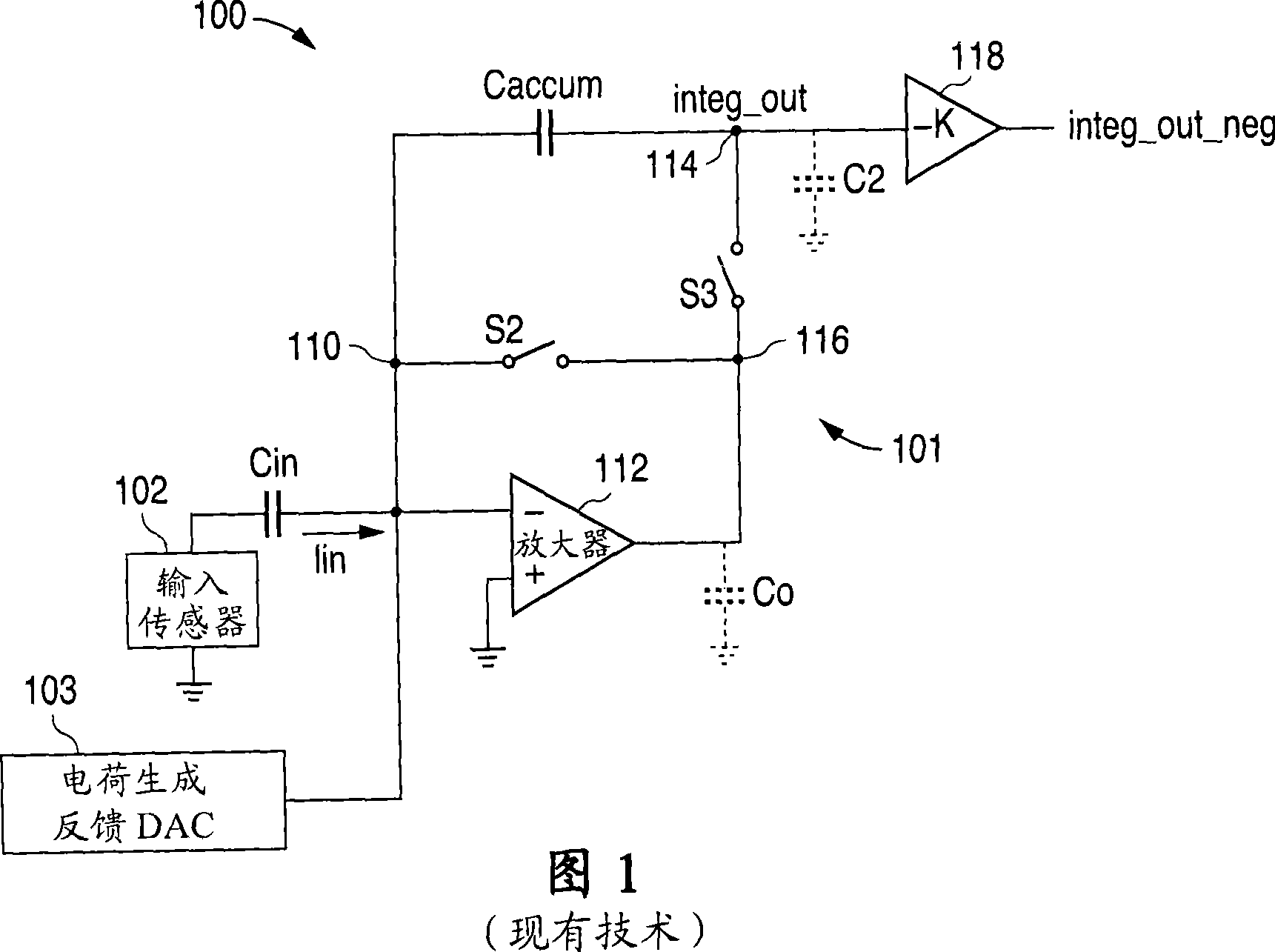
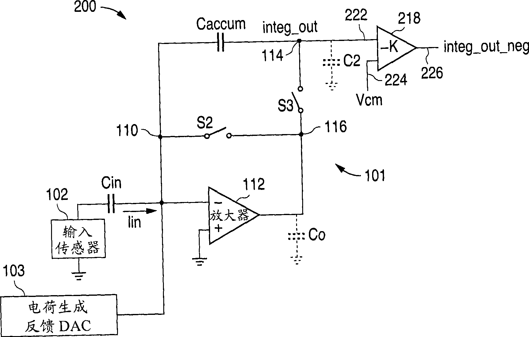
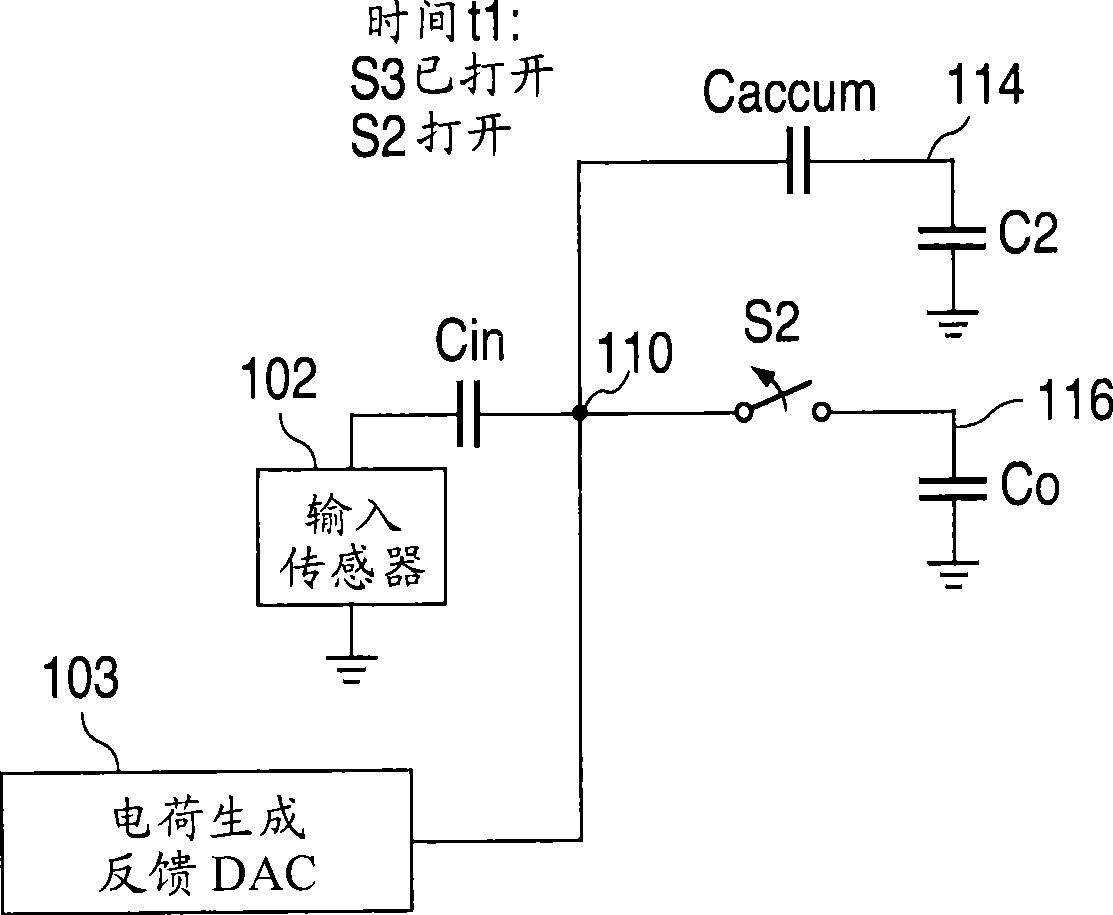
[0021] In particular, the low input capacitance buffer circuit of the present invention has particular application in analog-to-digital converters (ADCs), especially current-input ADCs that receive low-level input currents to be digitized. The buffer circuit of the present invention can be coupled with an integrator to form a charge balancing regul...


PUM


Abstract

A method for charge balancing in a current input ADC including maintaining a low capacitance value at the integrator output node where the capacitance value is independent of the integrator output voltage and operating conditions, generating a first voltage pedestal at a first active device switch at the end of the autozero phase having a first voltage polarity and a first magnitude, generating a second voltage pedestal at a second active device switch at the end of the integration phase having an opposite voltage polarity and the first magnitude, and summing the first voltage pedestal with the second voltage pedestal. The difference between the first voltage pedestal and the second voltage pedestal results in a net voltage error. The first and second voltage pedestals have the first magnitude under all operating conditions of the modulator and the two voltage pedestals cancel to yield a small net voltage error.

Description

[0001] Cross References to Related Applications [0002] This application is related to the following commonly assigned and concurrently filed U.S. Patent Application Serial No. 11 / 679,053, Jun Wan and Peter R. Holloway, entitled "LowCurrent Offset Integrator with Signal Independent Low InputCapacitance Buffer Circuit," which The patent application is hereby incorporated by reference in its entirety. technical field [0003] The present invention relates to a method in a current-input analog-to-digital converter (ADC), and more particularly to a method for charge balancing in a current-input ADC. Background technique [0004] An analog-to-digital converter is used to convert or digitize an analog input signal to produce a digital output signal that represents the value of the analog input signal within a given conversion time. A current-input ADC refers to an ADC that receives a low-level input current as an analog input signal to be digitized. Current input ADCs are also ...

Claims


Application Information

Patent Timeline
Patent Type & Authority Applications(China)
IPC IPC(8): H03M1/06H03M1/12
CPCH03M1/0607H03F2203/45212H03F2200/264H03F3/45179H03F3/45766H03F2203/45352H03F3/45475H03F2203/45342H03F3/45183H03F2203/45136H03M1/12
Inventor 万隽彼得·R·霍洛韦
Owner NAT SEMICON CORP
Why Eureka
Try Eureka