Waste water processing method

A waste water treatment, waste water technology, applied in the direction of water/sewage treatment, water/sludge/sewage treatment, separation method, etc., can solve the problem of high cost of waste water treatment, and achieve the effect of cost reduction, cost reduction, and simple waste water treatment process

Inactive Publication Date: 2009-04-01
SEMICON MFG INT (SHANGHAI) CORP
View PDF1 Cites 0 Cited by
  • Summary
  • Abstract
  • Description
  • Claims
  • Application Information

AI Technical Summary

Problems solved by technology

[0005] The invention provides a wastewater treatment method, which solves the problem of high wastewater treatment cost in the prior art

Method used


Image

  • Waste water processing method
  • Waste water processing method
  • Waste water processing method

Examples


Embodiment Construction

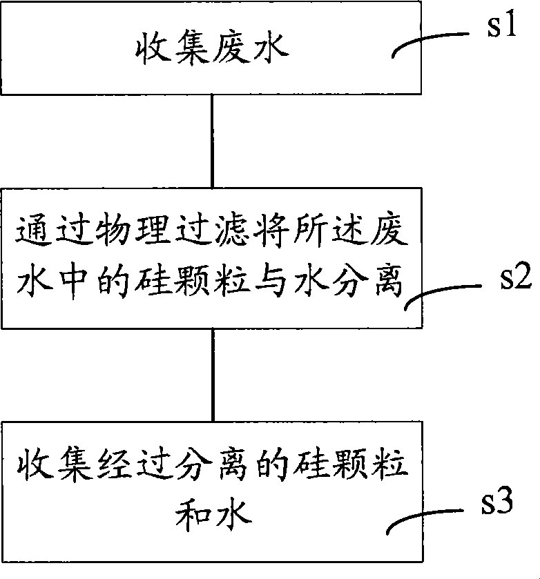
[0027] The waste water treatment method of the invention separates silicon particles and water in the waste water through physical filtration without adding chemicals, so that the waste water treatment process is simple and the cost is reduced.

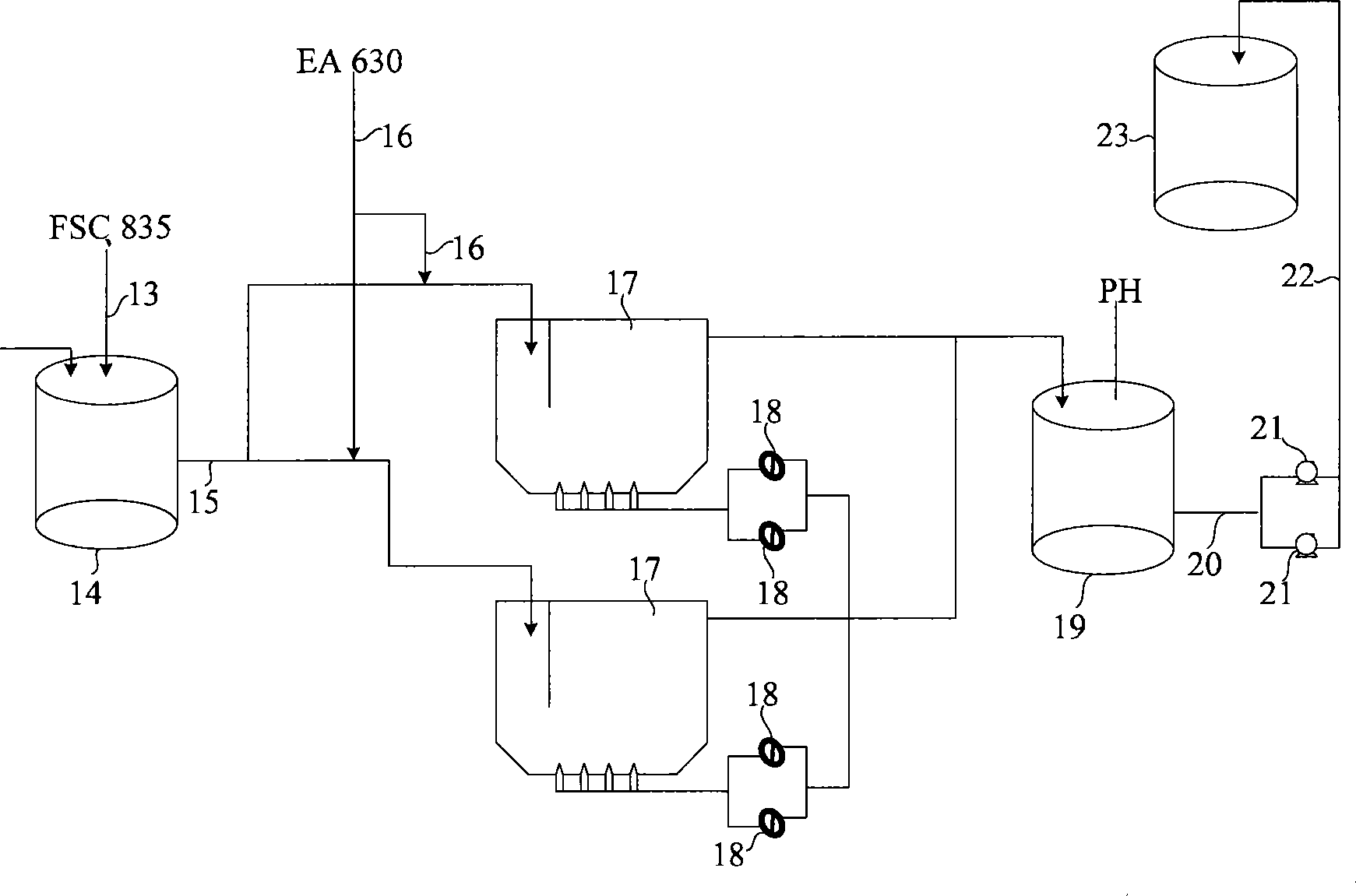
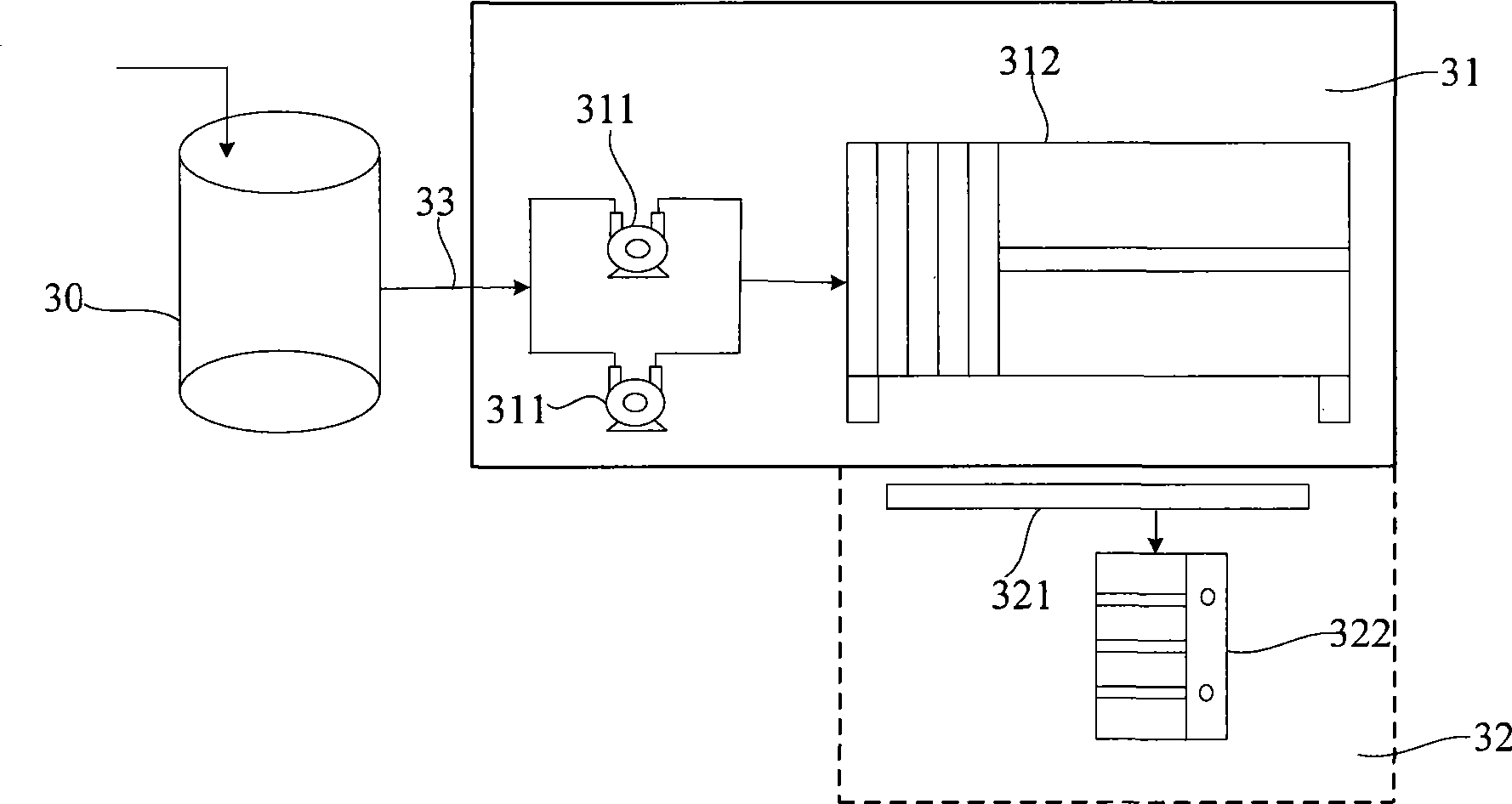
[0028] As mentioned above, before the semiconductor chip is packaged, the back of the semiconductor wafer needs to be thinned and the semiconductor chip is cut off from the semiconductor wafer, and then a single or several semiconductor chips are packaged, wired and tested. The backside thinning process is a process of removing part of the silicon material on the backside of the semiconductor wafer by grinding equipment. For example, for a 300mm semiconductor wafer, its thickness is generally 700 to 800mm, and it usually needs to be thinned to 200 to 400mm before packaging; The dicing process cuts semiconductor chips from semiconductor wafers by using a dicing saw with a diamond blade. No matter in the grinding or cutting process, a l...


PUM


Abstract

The invention provides a method of wastewater disposal, comprising the steps: the waste water is collected; silicon granules in the waste water are separated from water by physical filtration; the separated silicon granules and the water are collected. As the problem of higher cost on wastewater disposal of the prior art is solved by the method, the cost on wastewater disposal is saved.

Description

technical field [0001] The invention relates to a wastewater treatment method for grinding and scribing in a semiconductor packaging and testing process. Background technique [0002] In semiconductor manufacturing technology, semiconductor chips with various functions are formed through a series of processes such as photolithography, etching, deposition, ion implantation, grinding, cleaning, etc., and then the semiconductor chips are packaged and electrically tested, and finally form the end product. Currently, semiconductor chips are generally fabricated on silicon-based semiconductor wafers. Before packaging, firstly, the thickness of the semiconductor wafer needs to be reduced by milling; and then each semiconductor chip is cut from the semiconductor wafer by dicing. A large amount of industrial waste water is produced in the process of grinding and scribing, and the waste water contains suspended silicon and a small amount of grinding agent. Existing wastewater treat...

Claims


Application Information

Patent Timeline
IPC IPC(8): B01D37/00C02F1/00
Inventor 林信才李姿娴刘江冯均
Owner SEMICON MFG INT (SHANGHAI) CORP
Why Eureka
Try Eureka