
Reflection-permeation array substrate
An array substrate and array technology, applied in the field of anti-transmission array substrates, can solve problems such as difficulty in setting, achieve the effect of improving quality and simplifying manufacturing engineering
- Summary
- Abstract
- Description
- Claims
- Application Information
AI Technical Summary
Problems solved by technology
Method used
Image

Examples
no. 1 example
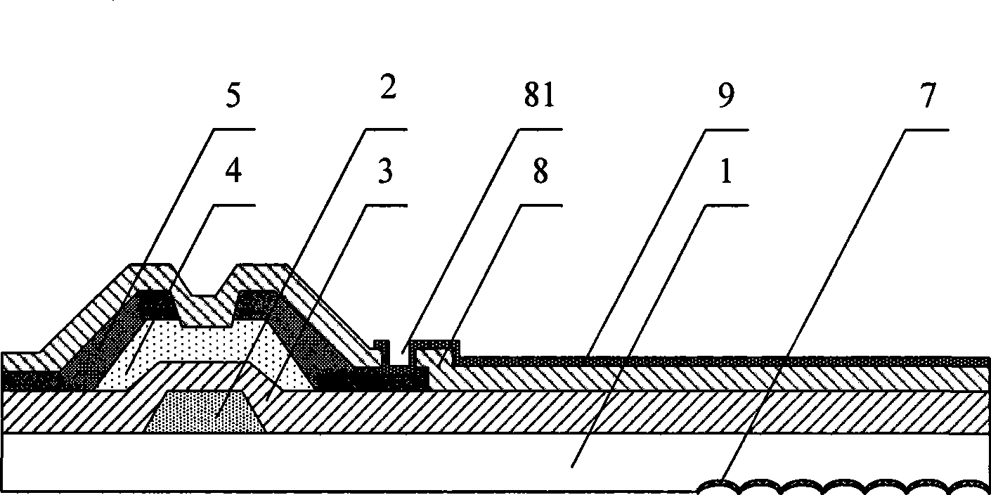
[0028] figure 2 It is a structural schematic diagram of the first embodiment of the present invention. like figure 2 As shown, the anti-transmissive array substrate includes: a glass substrate 1 and an array body, wherein the glass substrate 1 is provided with a transmissive area and a reflective area, and embossing is formed on the first surface of the glass substrate 1 corresponding to the reflective area, and the embossing is The second surface of the glass substrate 1 is recessed, and a reflective plate 7 with uniform thickness is arranged on the embossing of the first surface of the glass substrate 1. The shape of the reflective plate 7 is the same as the embossed shape; An array main body is arranged on the second face of the opposite glass substrate 1, wherein the array main body includes a gate line (not shown in the figure), a gate electrode 2, a gate insulating layer 3, an active layer 4, a source-drain electrode 5, a data line (not shown in the figure), passivat...
no. 2 example
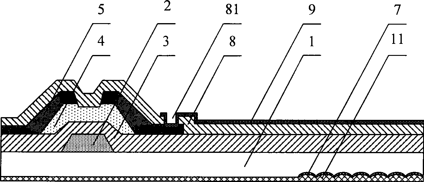
[0035] image 3 It is a structural schematic diagram of the second embodiment of the present invention. like image 3 As shown, the anti-transmissive array substrate includes: a glass substrate 1 and an array body, wherein the glass substrate 1 is provided with a transmissive area and a reflective area, and embossing is formed on the first surface of the glass substrate 1 corresponding to the reflective area, and the embossing is The structure is recessed to the second surface of the glass substrate 1, and a reflective plate 7 with uniform thickness is provided on the embossing of the first surface of the glass substrate 1. The shape of the reflective plate 7 is the same as that of the embossed shape, and a protective plate film 11, and the protective film 11 evenly covers the first surface of the glass substrate 1; the second surface of the glass substrate 1 opposite to the first surface of the glass substrate 1 is provided with an array body, wherein the array body includes...
no. 3 example
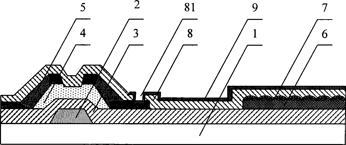
[0039] Figure 4 It is a structural schematic diagram of the third embodiment of the present invention. like Figure 4 As shown, the anti-transmissive array substrate includes: a glass substrate 1 and an array body, wherein the glass substrate 1 is provided with a transmissive area and a reflective area, and embossing is formed on the first surface of the glass substrate 1 corresponding to the reflective area, and the embossing is The second surface of the glass substrate 1 is recessed, and a reflective plate 7 with uniform thickness is arranged on the embossing of the first surface of the glass substrate 1. The shape of the reflective plate 7 is the same as the embossed shape; An array main body is arranged on the second face of the opposite glass substrate 1, wherein the array main body includes a gate line (not shown in the figure), a gate electrode 2, a gate insulating layer 3, an active layer 4, a source-drain electrode 5, a data line (not shown in the figure), passivat...
PUM
 Abstract
Description
Claims
Application Information