Milling processing device for wafer

A technology for grinding and wafer processing, which is applied in the field of grinding and processing devices to achieve the effect of suppressing the loss of working time and human error

Inactive Publication Date: 2009-04-08
DISCO CORP
View PDF2 Cites 20 Cited by
  • Summary
  • Abstract
  • Description
  • Claims
  • Application Information

AI Technical Summary

Problems solved by technology

In this way, it is not easy for anyone to adjust the inclination of the grinding member, but proficiency is required

Method used


Image

  • Milling processing device for wafer
  • Milling processing device for wafer
  • Milling processing device for wafer

Examples


Embodiment Construction

[0032] One embodiment of the present invention will be described below with reference to the drawings.

[0033] [1] Semiconductor wafer

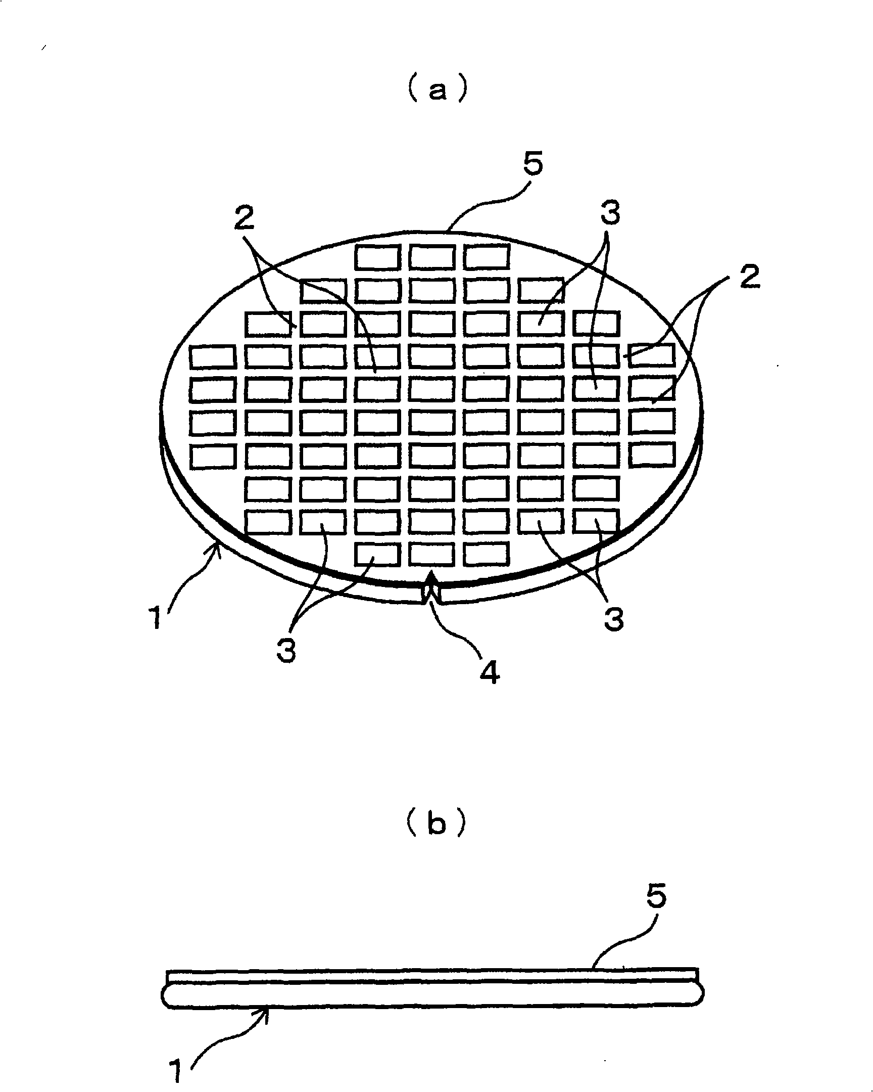
[0034] figure 1 Reference numeral 1 in FIG. 2 is a disk-shaped semiconductor wafer (hereinafter simply referred to as a wafer) whose back surface is ground and thinned by the grinding apparatus of one embodiment shown in FIG. 2 . The wafer 1 is a silicon wafer or the like, and its thickness before processing is, for example, about 700 μm. The surface of the wafer 1 is divided into a plurality of rectangular semiconductor chips 3 by grid-like dividing lines 2 . Electronic circuits (not shown), such as ICs and LSIs, are formed on the surfaces of these semiconductor chips 3 . In addition, a V-shaped notch (notch) 4 indicating the crystal orientation of the semiconductor is formed at a predetermined position on the peripheral surface of the wafer 1 . The wafer 1 is finally cut and divided along the planned dividing line 2 to be separated int...


PUM


Abstract

The invention provides a wafer grinding apparatus. In a grinding apparatus grinding the back of the wafer, the modulation of the inclination of the rotational axis of the grinding component to improve the productivity effect and wafer quality. The wafer grinding apparatus is provided with a slope regulation mechanism (100) for sloping the rotational axis (30a) of the grinding unit (30), and a grinding condition storage component (110) for storing angular adjustment values corresponding to the various grinding conditions. The grinding conditions of the wafer (1) are selected by the grinding condition storage component (110), so as to read the angular adjustment values of the grinding unit (30). A fore and after modulating liner (101) and a left-right modulating liner (105) of the slope regulation mechanism (100) are according to the angular adjustment values, so that the grinding unit is modulated to a slope angle corresponding to the grinding condition of the wafer. After the angle of the grinding unit is adjusted, the grinding unit is used to grind the wafer to get a wafer with the desired thickness.

Description

technical field [0001] The present invention relates to a grinding device for grinding and thinning a wafer, and more particularly to a grinding device capable of adjusting the angle of a grinding surface of a grinding member for grinding a wafer. Background technique [0002] A semiconductor chip on which an electronic circuit such as IC (Integrated Circuit) or LSI (large scale integration) is formed on the surface is now necessary for miniaturization of various electric and electronic devices. A semiconductor chip is manufactured by dividing a grid-like rectangular area on the surface of a disk-shaped semiconductor wafer (hereinafter referred to as wafer) by lines to cut called streets, and forming electronic circuits on these rectangular areas. , and then cut the wafer along the spacer lanes for segmentation. [0003] In such a manufacturing process, before the wafer is divided into semiconductor chips, the wafer is thinned to a predetermined thickness by grinding the ba...

Claims


Application Information

Patent Timeline
Patent Type & Authority Applications(China)
IPC IPC(8): B24B7/20
Inventor 沟本康隆堤义弘
Owner DISCO CORP
Why Eureka
Try Eureka