Semiconductor device

A semiconductor and device technology, applied in the field of semiconductor devices, can solve the problems of difficult maintenance, easily damaged gate leads of gate commutated thyristors, complicated assembly of semiconductor devices, etc., and achieve the effects of simple installation and maintenance, and convenient replacement and maintenance.

Active Publication Date: 2010-06-09
ZHUZHOU CRRC TIMES SEMICON CO LTD
View PDF5 Cites 0 Cited by
  • Summary
  • Abstract
  • Description
  • Claims
  • Application Information

AI Technical Summary

Problems solved by technology

[0006] However, when the above-mentioned semiconductor device formed by combining the gate commutation thyristor and the printed circuit board is combined, the gate commutation thyristor needs to be screwed into the mounting hole by rotating; or the gate commutation thyristor is installed in one of the half After the circular groove', the other two semicircular grooves are connected to the previous semicircular groove, which makes the assembly of the above-mentioned semiconductor devices more complicated and difficult to maintain
It is also easy to damage the gate lead and / or auxiliary cathode lead of the gate commutated thyristor during assembly or disassembly

Method used


Image

  • Semiconductor device
  • Semiconductor device
  • Semiconductor device

Examples


Embodiment 1

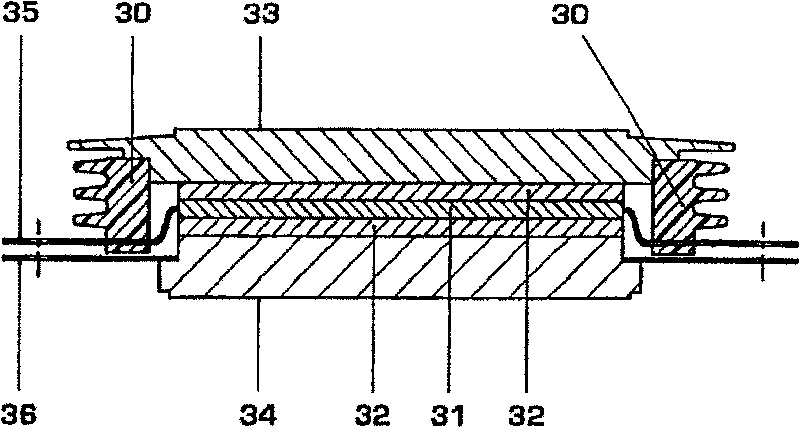
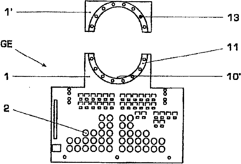
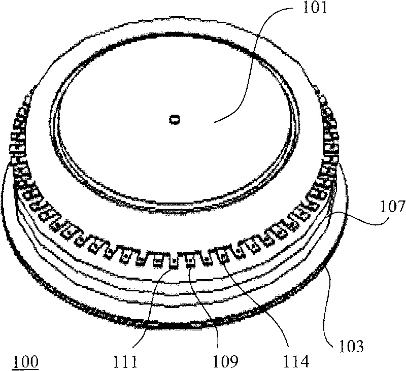
[0049] Figure 6 is an exploded view of the first embodiment of the semiconductor device of the present invention. image 3 and Figure 4 It is a side view of a gate commutated thyristor in the first embodiment of the semiconductor device of the present invention. Figure 5 It is a schematic cross-sectional view of a gate-commutated thyristor in the first embodiment of the semiconductor device of the present invention. Figure 7 It is a plan view of part of the printed circuit board of the semiconductor device of the present invention.

[0050] Please refer to Figure 6 , the semiconductor device includes a gate commutated thyristor 100 and a printed circuit board 300 .

[0051] Please refer to image 3 , 4 and Figure 5 , the gate commutated thyristor 100 includes an anode terminal 103 , a cathode terminal 101 , and a casing 105 between the anode terminal 103 and the cathode terminal 101 . The gate commutation thyristor 100 also includes a welding skirt 104 located at t...

Embodiment 2

[0080] Such as Figure 9 and Figure 10 As shown, the fastening structure may also include positioning holes (not marked) on the gate lead 111 and / or cathode lead 109, via holes corresponding to the positioning holes on the printed circuit board 300, and fixing pins 308, alternately insert positioning pins 310 into the positioning holes on the gate lead 111 and the cathode lead 109 (eg Figure 10 shown) and fixing pin 308 (as Figure 9 As shown), the position corresponding to the positioning hole on the printed circuit board 300 has such as Figure 11 The via hole 303 and the positioning slot 307 are shown, and the positioning pin 310 and the fixing pin 308 pass through the corresponding via hole 303 and the positioning slot 307 .

[0081] In addition, an insulating strip 304 may also be provided between the pressure strip 301 and the gate lead 111 and the cathode lead 109 . No more details here.

[0082] Other aspects of the second embodiment are the same as those of the...


PUM


Abstract

A semiconductor device comprises a gate commutated thyristor and a printed circuit board. The gate commutated thyristor comprises an anode terminal (103), a cathode terminal (101), a tube shell (105)and a gate lead (111) led from the outer wall of the tube shell (105); the gate lead (111) is provided with a mounting surface (112); the printed circuit board comprises a mounting hole (302) and a first contact electrode; the gate commutated thyristor is inserted into the mounting hole (302) of the printed circuit board and causes the mounting surface (112) to contact with the first contact electrode; the gate commutated thyristor also comprises a cathode lead (109) which is led from the outer wall of the tube shell (105) and is electrically connected with the cathode terminal (101); a secondcontact electrode is also arranged around the mounting hole and on the same side as the first contact electrode; the cathode lead (109) is provided with a mounting surface, and the mounting surface (110) of the cathode lead is in contact with the second contact electrode. The semiconductor device is easy to be assembled.

Description

technical field [0001] The invention relates to the technical field of power semiconductors, in particular to a semiconductor device including a gate commutation thyristor. Background technique [0002] Integrated Gate Commutated Thyristors (IGCT) are fully-controlled power semiconductor devices used in power electronic devices. It is a device composed of a gate-commutated thyristor (GCT, also known as a gate-controlled thyristor) and a gate control unit. Usually, the gate control unit is located on the printed circuit board, and the GCT is connected to the gate control unit through the interface circuit on the printed circuit board. [0003] In the Chinese patent application document with the publication number CN1292150A, a controlled gate-controlled thyristor and a semiconductor device (referred to as a component in the patent application document) formed by connecting it to a printed circuit board are disclosed. figure 1 It is a cross-sectional view of one embodiment o...

Claims


Application Information

Patent Timeline
Patent Type & Authority Patents(China)
IPC IPC(8): H01L23/488H05K1/18
Inventor 张明李继鲁蒋谊陈芳林邹昌彭华文
Owner ZHUZHOU CRRC TIMES SEMICON CO LTD
Why Eureka
Try Eureka