

Method for cleaning abnormal residual on wafer rear surface after Cu CMP procedure
A back surface, wafer technology, applied in the field of cleaning, can solve problems such as corroded metal, wafer damage, corrosion, etc., to achieve the effect of improving yield
- Summary
- Abstract
- Description
- Claims
- Application Information
AI Technical Summary
Problems solved by technology
Method used
Image

Examples
Embodiment Construction
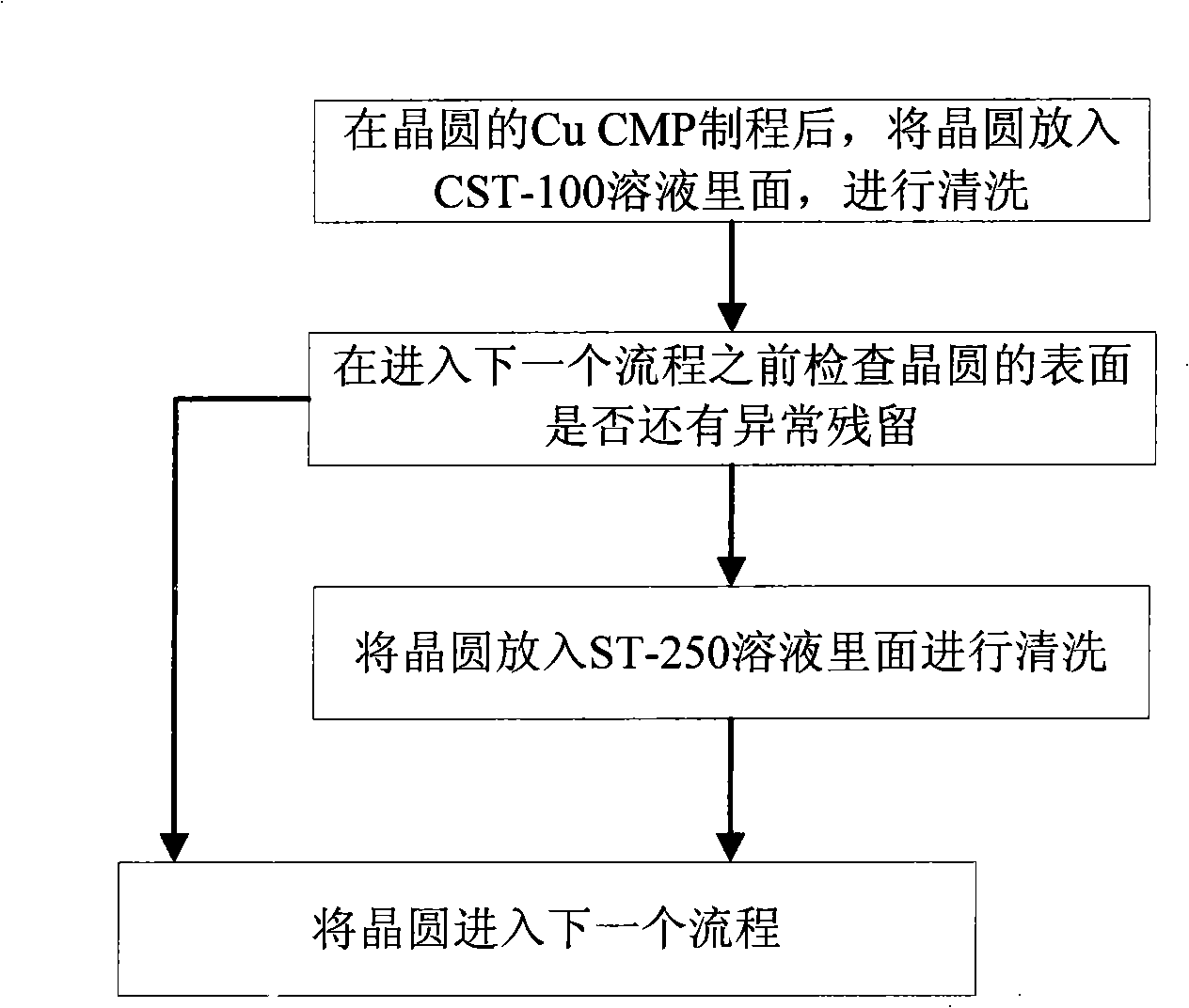
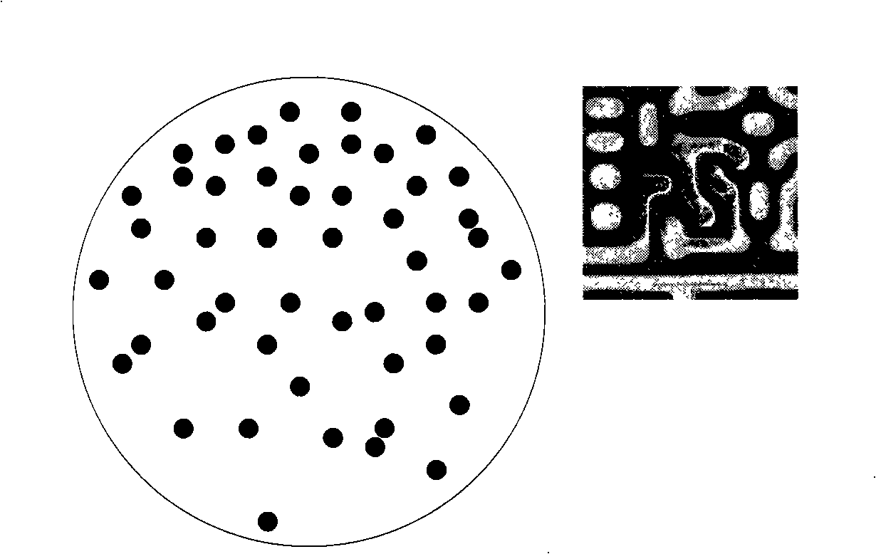
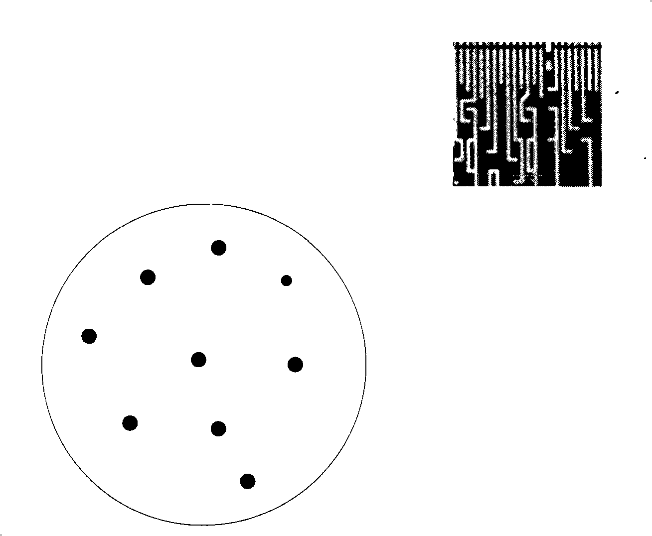
[0017] The present invention is a further improvement to the existing cleaning method, that is, after the Cu CMP process of the wafer, first use the CTS-100 solution to clean the wafer, and check the wafer before entering the next process, if If the wafer is not oxidized and has no impurities on the surface, it will directly enter the next process. If there are abnormal residual impurities on the surface of the wafer, the wafer needs to be further processed, that is, to be cleaned again before entering the next process. And the present invention just makes great improvement to the cleaning liquid in this process, and what this cleaning liquid uses is a kind of new alkaline cleaning liquid, and its pH value is in the scope of 7~9 about, like this again to crystal When cleaning the circle, because the cleaning solution is weakly alkaline, it is difficult for the cleaning solution to react with metal oxides, let alone corrode the metal, and it is easy to clean away other impuritie...
PUM
 Abstract
Description
Claims
Application Information